Electronic device and RF module

a technology of electronic devices and modules, applied in the field of electronic devices, can solve the problems of increasing circuit area, affecting power efficiency, and difficulty in reducing or costing, so as to prevent the deterioration of power efficiency due to impedance mismatching and reduce the reflection of signals

Inactive Publication Date: 2008-06-12
RENESAS ELECTRONICS CORP
View PDF3 Cites 106 Cited by
  • Summary
  • Abstract
  • Description
  • Claims
  • Application Information

AI Technical Summary

Benefits of technology

[0097]In an RF module according to a specific embodiment, the output matching circuit is provided for reducing the signal reflection due to the difference between the output impedance for generating the output ampl...

Problems solved by technology

However, when various filter circuits or the like are configured by combining the spiral inductor and the capacitor disclosed in the Patent Document 1 and the Patent Document 2, since the circuit area increases and about ten layers of wiring substrates are required in some cases for the layout of the wirings, downsizing or cost reduction is difficult to be achieved.
However, since the inductor can be formed in only two layers, the inductance is insufficient, and therefore, it can be applied o...

Method used


Image

  • Electronic device and RF module
  • Electronic device and RF module
  • Electronic device and RF module

Examples


first embodiment

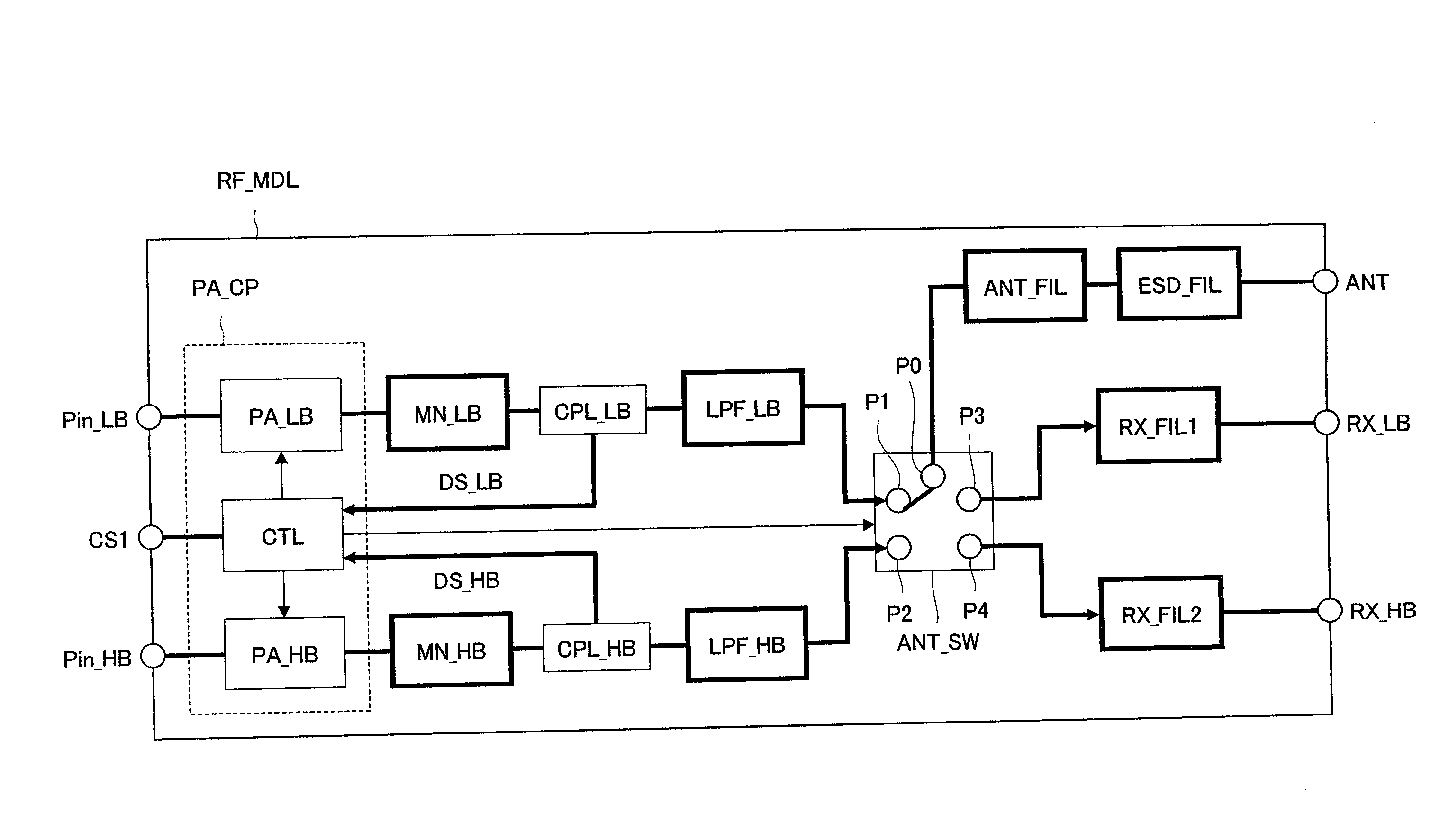
[0121]FIG. 1 is a block diagram showing an example of the configuration of an RF module according to a first embodiment of the invention. An RF module (radio frequency power amplifying module) of the first embodiment is used in, for example, a mobile communication device such as a cellular telephone and is designed to support both of a low frequency band and a high frequency band. For example, the low band includes GSM (Global System for Mobile Communication) 850 or GSM 900 or the like, and the high band includes GSM 1800 or GSM 1900. Here, GSM means a standard of a wireless communication protocol used in the digital mobile phones. GSM includes four available radio wave frequency bands, and a band of 900 MHz (880 to 960 MHz) is referred to as GSM900 or simply as GSM. Also, a band of 1800 MHz (1710 to 1880 MHz) is referred to as GSM1800, DCS1800 or PCN. Also, a band of 1900 MHz (1850 to 1990 MHz) is referred to as GSM1900, DCS1900, or PCS (Personal Communication Services). GSM1900 is...

second embodiment

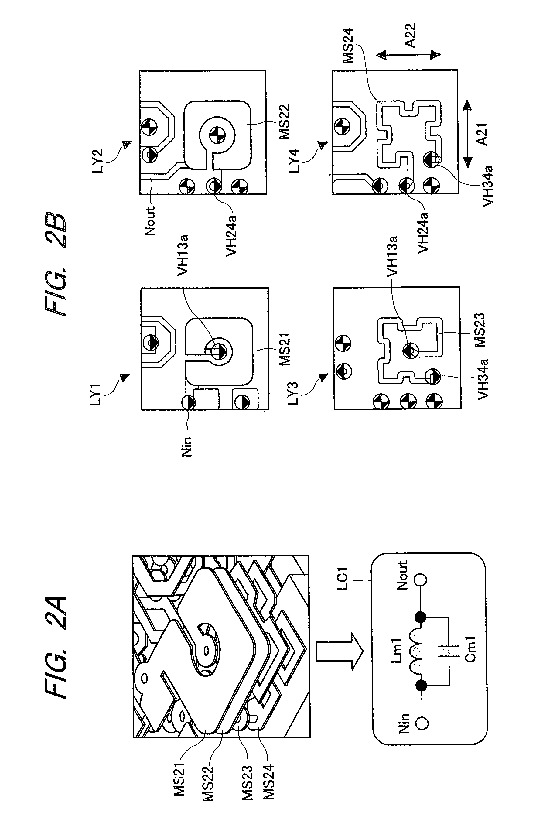
[0143]In the second embodiment, an example of a configuration of a resonant circuit, which is used in the various filter circuits and the output matching circuits shown in FIG. 1 but is different from the that shown in FIG. 2A and FIG. 2B, will be described. FIG. 5 shows an example of the configuration of a resonant circuit according to the second embodiment of the present invention, in which FIG. 5A is a perspective view of the resonant circuit and FIG. 5B is a plan view illustrating the respective layers shown in FIG. 5A. Similar to that shown in FIG. 2A and FIG. 2B, the resonant circuit shown in FIG. 5A and FIG. 5B is achieved by using, for example, a four layered multilayer wiring substrate including a first wiring layer LY1 to a fourth wiring layer LY4, and the rear surface of LY4 serves as a ground electrode.

[0144]Wiring patterns MS31 and MS32 each of which is formed from an approximately loop-shaped line are formed in LY1 and LY2. Wiring patterns (electrode pattern) MS33 and ...

third embodiment

[0153]In the third embodiment, a configuration example in the case where the parallel resonant circuit LC1 in FIG. 2A and FIG. 2B and the parallel resonant circuit LC2 in FIG. 5A and FIG. 5B are applied to the RF module in FIG. 1 will be described in detail. FIG. 8 is a circuit diagram showing an example of a configuration in an RF module according to the third embodiment of the present invention. In the RF module shown in FIG. 8, as described in FIG. 1, an output from the power amplifier circuit PA_LB for low band is transmitted to the antenna switch circuit ANT_SW via the output matching circuit MN_LB, the coupler circuit CPL_LB, the low-pass filter circuit LPF_LB and the capacitor Cs13. Here, the output of PA_LB formed in a semiconductor chip is connected to MN_LB formed on the wiring substrate via a bonding wire or the like. Further, Cs13 is a capacitor for cutting direct current and is formed from, for example, SMD components.

[0154]PA_LB is, for example, an amplifier circuit ha...


PUM


Abstract

A parallel resonant circuit is realized by stacking first to fourth wiring patterns each having at least an inductance element. One of the adjacent first and second wiring patterns is set to a signal input node and the other thereof is set to a signal output node. Then, the signal input node is connected to the signal output node via inductance elements of the first wiring pattern, third wiring pattern, fourth wiring pattern and second wiring pattern in order. By adjacently forming wiring layers of the signal input and output nodes, a capacitance value between the input and output nodes is increased compared to that when they are separated. Also, by increasing the line width of the first and second wiring patterns, the capacitance value can be further increased. Therefore, it is possible to achieve a large capacitance value in a small area and downsizing of the electronic device.

Description

CROSS-REFERENCE TO RELATED APPLICATION[0001]The present application claims priority from Japanese Patent Applications No. 2006-331358 filed on Dec. 8, 2006, No. 2007-22606 filed on Feb. 1, 2007 and No. 2007-295938 filed on Nov. 14, 2007, the contents of which are hereby incorporated by reference into this application.TECHNICAL FIELD OF THE INVENTION[0002]The present invention relates to an electronic device. In particular, it relates to a technique usefully applied to a radio frequency module (RF module) including filters and the like for reducing radio frequency distortion.BACKGROUND OF THE INVENTION[0003]Several communication protocols are available for mobile communication typified by mobile phones. For example, in Europe, in addition to GSM and EDGE which provides an increased data communication speed of GSM prevailing as a second-generation wireless communication protocol, W-CDMA, the service of which has recently started, is available as a third-generation wireless communicati...

Claims


Application Information

Patent Timeline
IPC IPC(8): H03H7/00H04B1/02
CPCH01F17/0006H03H7/0115H01L2924/0002H03H7/1758H03H7/1766H03H7/383H03H7/465H03H2001/0085H05K1/0237H05K1/116H05K1/16H05K1/165H05K3/429H05K2201/09636H05K2201/09672H01L2924/00
Inventor TAKAHASHI, WATARUTSUCHIDA, SHIGERUOKABE, HIROSHI
Owner RENESAS ELECTRONICS CORP
Why Eureka
Try Eureka