Apparatus and method for reducing dark current

Inactive Publication Date: 2008-06-12
ALTASENS
View PDF5 Cites 37 Cited by
  • Summary
  • Abstract
  • Description
  • Claims
  • Application Information

AI Technical Summary

Benefits of technology

[0019]In general, the present invention is an apparatus, method and image sensor that reduces the dark current in each pixel. More particularly, in one embodiment of the present invention, the negative potential barrier at the transfer gate of each pixel in an image sensor is raised when the photodetector is integrating (when the transfer gate is “off”) to thereby eliminate dark current generation in this region. The potential barrier is applied via a circuit structure that is capable of handling a strongly negative voltage. The circuit structure also serves as a conduit for conducting a strongly positive voltage to minimize the potential barrier during signal transfer and readout.
[0020]In one embodiment, a plurality of pixels connected via a bus to a transfer driver gate transistor. Each pixel comprises a pinned photodiode. The transf

Problems solved by technology

Although other drawbacks have been successively accommodated by camera designers, the key CCD disadvantage that has become a major technical barrier over the past 5 years and reinvigorated competition is excess white noise at video rates above 20 MHz.
Specifically, the emergence of high resolution digital still cameras (DSC) and high definition television has exposed the fact that CCD output amplifier noise increases rapidly and is excessive at video rates above about 20 MHz.
Thus, it is impractical to use CCDs for the latest imaging products requiring maximum performance.
While CIS sensors have inherent performance advantages at high video rates, their best performance in visible light cameras has often been of lower quality (than the best CCD-based cameras operating at lower rates) due to the fact that the available CMOS processes were optimized for microprocessor and memory chips rather than high performance imaging sensors.
The former issue is fundamental to silicon due to mid-gap st

Method used


Image

  • Apparatus and method for reducing dark current
  • Apparatus and method for reducing dark current
  • Apparatus and method for reducing dark current

Examples


Embodiment Construction

[0031]The following description is provided to enable any person skilled in the art to make and use the invention and sets forth the best modes contemplated by the inventor for carrying out the invention. Various modifications, however, will remain readily apparent to those skilled in the art. Any and all such modifications, equivalents and alternatives are intended to fall within the spirit and scope of the present invention.

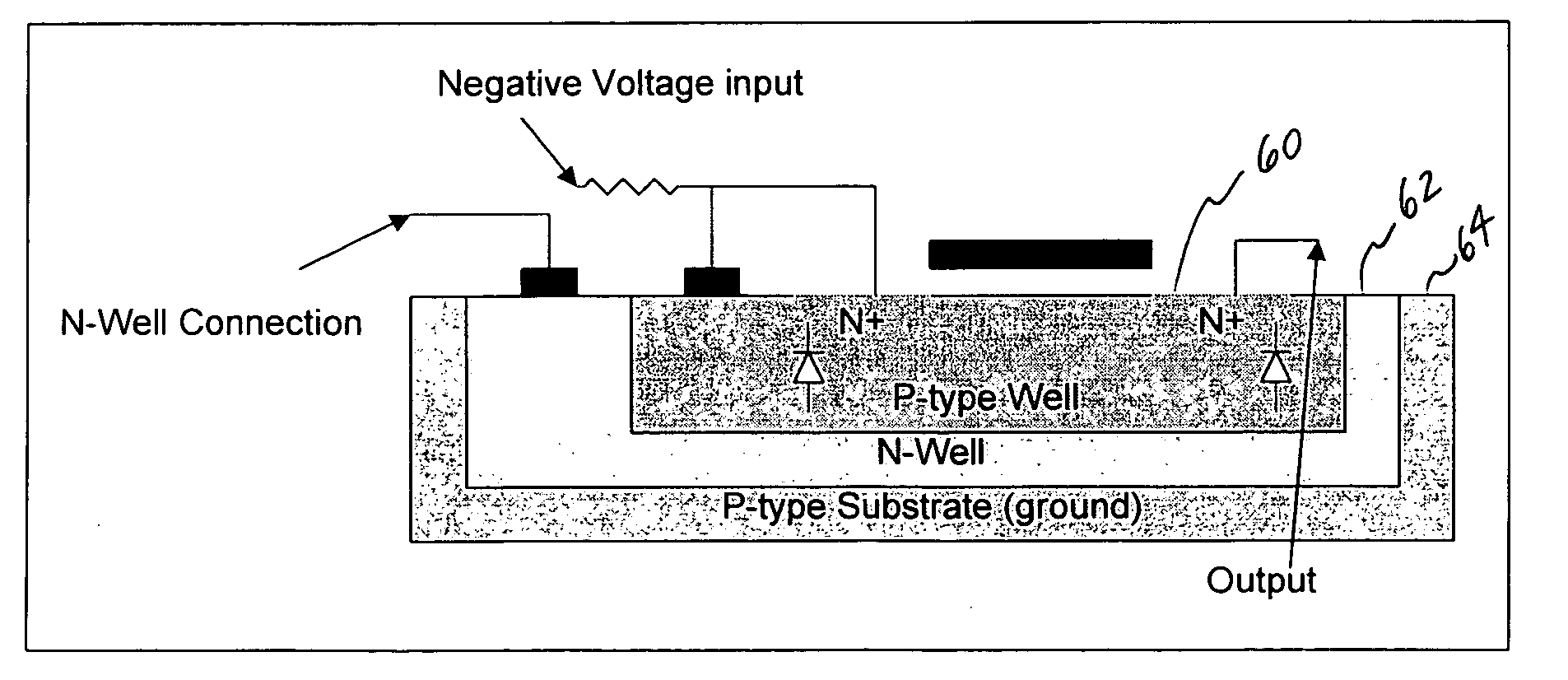
[0032]The present invention provides a system-on-chip solution that overcomes the disadvantages of the devices described in the prior art while maintaining or enhancing their favorable characteristics. The present invention is applicable to any active or passive pixel structures.

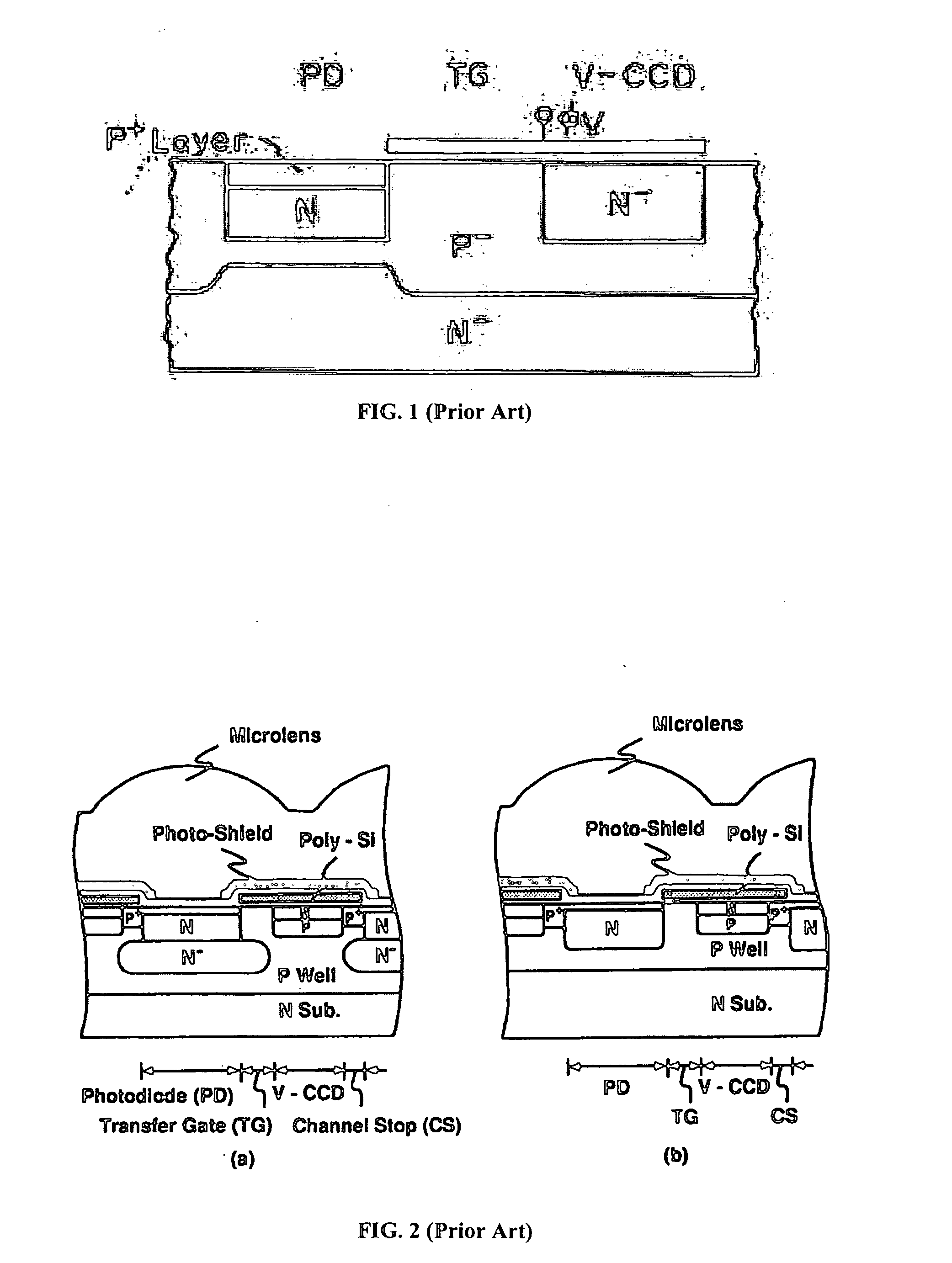
[0033]In pinned photodiode pixels, a large portion of the dark current is actually generated in the region near the transfer gate. The transfer gate is an electrically programmable barrier between the pinned photodiode and the floating diffusion which converts the photo-generated charge...


PUM


Abstract

An apparatus and method that reduces the dark current in each pixel of an image sensor, where each pixel has a pinned photodiode. A negative potential barrier at the transfer gate of each pixel is raised when the photodiode is integrating (when the transfer gate is “off”) to thereby eliminate dark current generation in this region. The potential barrier is applied via a “triple well” transistor circuit structure that is capable of handling a strongly negative voltage. The circuit structure also serves as a conduit for conducting a strongly positive voltage to minimize the potential barrier during signal transfer and readout, thereby reducing image lag.

Description

BACKGROUND OF THE INVENTION[0001]1. Field of the Invention[0002]The present invention relates generally to electronic imaging sensors, and more particularly, to an apparatus and method for reducing dark current.[0003]2. Description of the Related Art[0004]The two types of semiconductor-based imagers in widespread use today are charge coupled devices (CCD) and CMOS image sensors (CIS).[0005]Commercial cameras have largely relied on CCD imagers for the last 20 years. The key CCD advantage enabling dominance until now is the ability to produce high quality images at video rates up to about 20 MHz at satisfactory cost. Although other drawbacks have been successively accommodated by camera designers, the key CCD disadvantage that has become a major technical barrier over the past 5 years and reinvigorated competition is excess white noise at video rates above 20 MHz. Specifically, the emergence of high resolution digital still cameras (DSC) and high definition television has exposed the ...

Claims


Application Information

Patent Timeline
IPC IPC(8): H04N9/64
CPCH01L27/14643H01L27/14609
Inventor BLANQUART, LAURENTSHAH, JOEY
Owner ALTASENS
Why Eureka
Try Eureka