
Light Emitting Device and Method of Fabricating Light Emitting Device

a light emitting device and light-emitting technology, which is applied in the direction of manufacturing tools, soldering devices, and semiconductor/solid-state device details, etc., can solve the problem of inability to quickly solve the delamination problem of the au—sn-base solder layer, and achieve the effect of improving the light extraction efficiency, improving the corrosion resistance of the solder layer, and low reflectivity

Inactive Publication Date: 2008-07-10
SHIN-ETSU HANDOTAI CO LTD
View PDF7 Cites 21 Cited by
  • Summary
  • Abstract
  • Description
  • Claims
  • Application Information

AI Technical Summary

Benefits of technology

[0017]In the light emitting device of this invention described above, as a solder material used for mounting the second electrodes disposed on the mounting side of the compound semiconductor layer, the Au—Sn-base solder layer, mainly containing Au, and having the Sn content adjusted so as to achieve the melting point higher than that of the Sn-base solder layer but not higher than 500° C., is adopted. An essential feature of this invention resides in that the Sn-base solder layer, composed of the Sn-base metal mainly containing Sn and having the melting point lower than that of the alloyed contact layer, is disposed in between, rather than bringing the Au—Sn-base solder layer into direct contact with the alloyed contact layer (generally hard, such as Au—Ge alloy, Au—Be alloy and so forth described later) for lowering contact resistance in the second electrodes. The solder layer mainly containing Sn is not only excellent in adhesiveness with the Au—Sn-base solder layer, but also far softer as compared with the Au—Sn-base solder layer, allowing itself to function as a so-called buffer layer absorbing and moderating, by plastic deformation, any applied stress due to impact or thermal hysteresis. As a consequence, delamination of the Au—Sn-base solder layer and so forth can largely be suppressed.
[0031]That is, the alloyed contact layer is formed as being distributed on the second main surface of the compound semiconductor layer, and the Sn-base solder layer is formed so as to cover the alloyed contact layer and the exposed area of the compound semiconductor layer as background in an integrated manner. The Au—Sn-base solder layer is further formed, the Sn-base solder layer fusing annealing step is carried out, and thereafter the lift-off process is carried out so as to remove the stacked film of the Sn-base solder layer and the Au—Sn-base solder layer, selectively in the portion thereof covering the background of the alloyed contact layer, while leaving the portion thereof covering the alloyed contact layer as being closely adhered to the alloyed contact layer. In the Sn-base solder layer fusing annealing step, the adhesive force of the Sn-base solder layer with the compound semiconductor layer, specifically in the portion thereof in direct contact with the exposed region of the compound semiconductor layer, is far smaller than the adhesive force thereof with an underlying metal, specifically in the portion having the alloyed contact layer formed therein, so that the portion covering the background of the alloyed contact layer can extremely readily be lifted off, typically by adhering and peeling of an adhesive sheet. Structure of the resultant solder layer is such as having the circumferential side faces thereof formed as mechanically fractured surfaces extending in the thickness-wise direction as being originated from the outer circumference of the bonding interface with the alloyed contact layer.

Problems solved by technology

Investigations by the present inventors have, however, revealed that the problem of delamination of the Au—Sn-base solder layer cannot readily be solved, even if the configuration described in Patent Document 3 is adopted.
Patent Document 3 exemplifies poor adhesion between the Au—Sn-base solder layer and the Mo layer as a causal factor of the delamination, however in practice, it is supposed that, due to hardness and poor ductility of the Au—Sn-base solder layer per se, and also due to relatively poor ductility of the AuGe alloy as an object to be adhered to, the materials cannot absorb stress induced by impact or thermal hysteresis by their plastic deformation, and result in delamination.

Method used


Image

  • Light Emitting Device and Method of Fabricating Light Emitting Device
  • Light Emitting Device and Method of Fabricating Light Emitting Device
  • Light Emitting Device and Method of Fabricating Light Emitting Device

Examples


Embodiment Construction

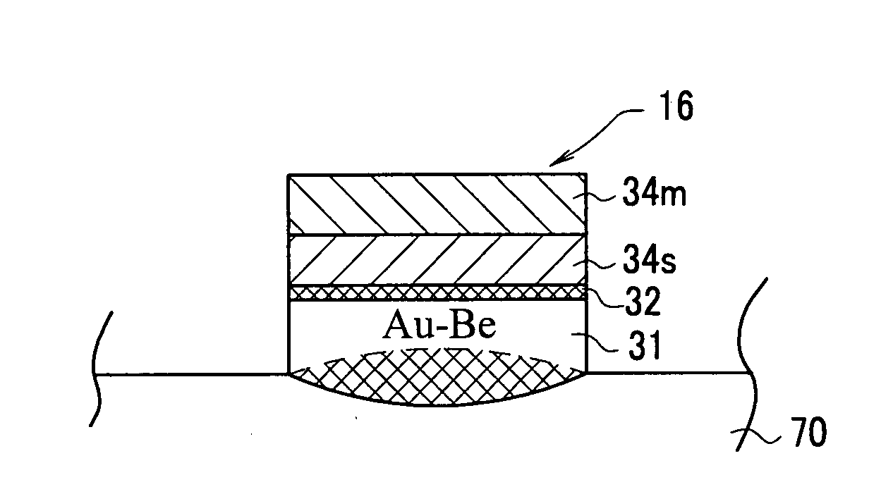
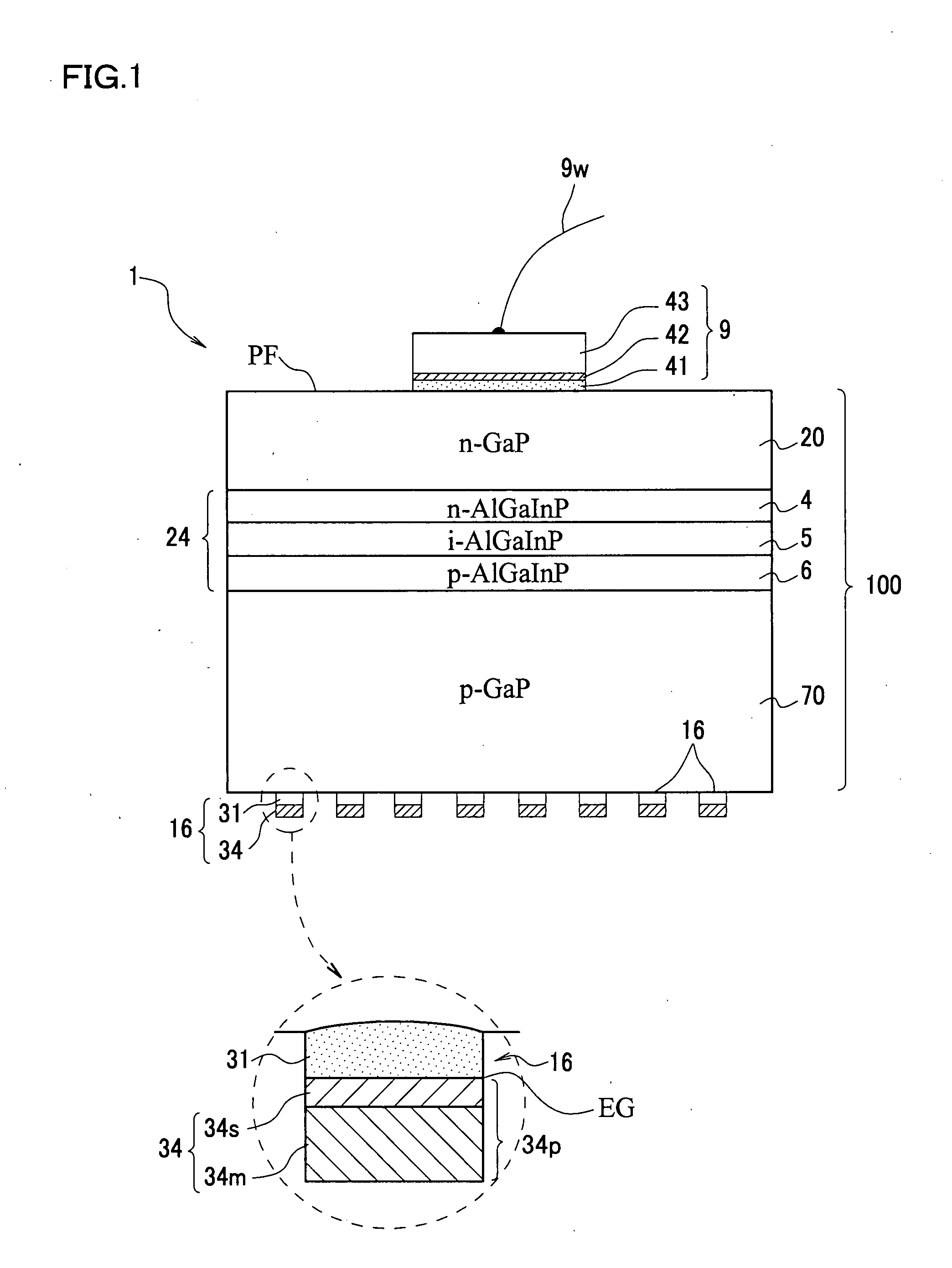
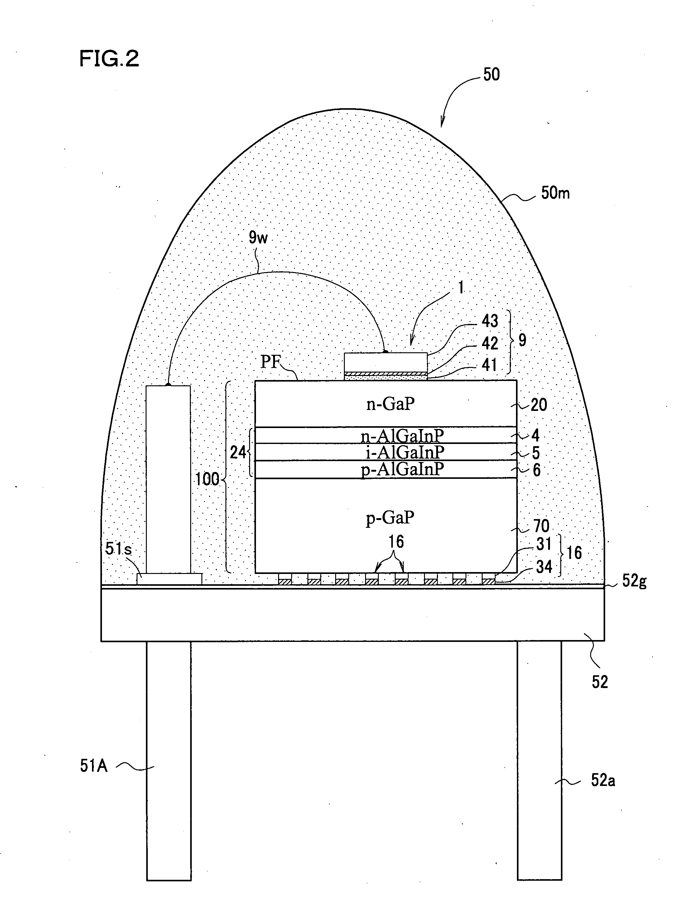
[0047]Embodiments of the method of fabricating the light emitting device of this invention will be explained below, referring to the attached drawings. FIG. 1 is a schematic view showing light emitting device to be applied with this invention. The light emitting device 1 has a compound semiconductor layer 100 having therein a light emitting layer section 24, and while assuming the main surface of the compound semiconductor layer 100 positioned on the light extraction side as a first main surface, and the main surface opposite thereto as a second main surface, has a first electrode 9 formed on the first main surface, and has second electrodes 16 formed on the second main surface, respectively. Each of the second electrodes 16 has an alloyed contact layer 31 disposed in contact with the second main surface of the compound semiconductor layer 100, aimed at reducing contact resistance with the compound semiconductor layer 100, and a solder layer 34 connecting the alloyed contact layer 3...


PUM

PropertyMeasurementUnit
melting pointaaaaaaaaaa
peak emission wavelengthaaaaaaaaaa
temperatureaaaaaaaaaa

Abstract

A second electrode (16) formed on a second main surface of a compound semiconductor layer (100) of a light emitting element (1) is arranged in contact with the second main surface of the compound semiconductor layer (100) and has a junction alloying layer (31) for reducing the resistance due to the junction with said compound semiconductor layer (100) and a solder layer (34) for connecting said junction metal layer to an electoconductive support (52). In the solder layer (34), there are formed an Sn-based solder layer (34s) which is arranged on the junction alloying layer (31) side and comprises an Sn-based metal containing Sn as a main component and having a melting point lower than that of the junction alloying layer (31) and an Au—Sn based solder layer (34m) which is arranged on the side opposite to the junction alloying layer (31) with respect to said Sn-based solder layer (34s) and in contact therewith and contains 30 to 90 mass % of Au and 10 to 70 mass % of Sn and has a total content of Au and Sn of 80 mass % or more and has a melting point higher than that of the Sn-based solder layer (34s). The above structure of an element is excellent in the reliability of the junction between an Au—Sn based solder layer and a junction alloying layer, which results in making the Au—Sn based solder layer less prone to exfoliation, in the case of a light-emitting element which adopts the mounting using an Au—Sn based solder layer.

Description

RELATED APPLICATIONS[0001]This application claims the priority of Japanese Patent Application No. 2005-023988 filed on Jan. 31, 2005, which is incorporated herein by reference.BACKGROUND OF THE INVENTION[0002]1. Field of the Invention[0003]This invention relates to a light emitting device and a method of fabricating the light emitting device.[0004]2. Description of the Related Art[0005][Patent Document 1] Japanese Laid-Open Patent Publication No. H2-260671[0006][Patent Document 2] Japanese Laid-Open Patent Publication No. H9-27498[0007][Patent Document 3] Japanese Laid-Open Patent Publication No. 2003-142731[0008][Non-Patent Document 1]“Development of Highly Reliable Sn—Ag Lead-Free Solder Alloy”, The R&D Review, Toyota Central Research Labs., Inc., Vol. 35, No. 2 (2000), p. 39”[0009]Light emitting devices composed of compound semiconductors have long been configured, while assuming the main surface thereof positioned on the light extraction side as a first main surface, and the mai...

Claims


Application Information

Patent Timeline
Patent Type & Authority Applications(United States)
IPC IPC(8): H01L33/00B23K31/02H01L33/38H01L33/30H01L33/40H01L33/56H01L33/62
CPCB23K1/0016B23K35/001H01L2224/45144H01L2924/01322H01L2933/0016H01L2924/3011H01L2924/01079H01L2924/01078H01L2924/01004B23K35/262B23K35/3013B23K2201/40H01L24/31H01L24/48H01L33/0079H01L33/30H01L33/382H01L33/40H01L33/62H01L2224/29144H01L2224/48091H01L2224/48137H01L2224/4823H01L2224/48463H01L2224/73257H01L2924/00014H01L2924/0105H01L2924/3512H01L2924/00H01L24/45H01L2924/181B23K2101/40H01L33/0093H01L2224/05599H01L2924/00012
Inventor IKEDA, HITOSHIOBARA, MASAYOSHI
Owner SHIN-ETSU HANDOTAI CO LTD
Features
  • Generate Ideas
  • Intellectual Property
  • Life Sciences
  • Materials
  • Tech Scout
  • Unparalleled Data Quality
  • Higher Quality Content
  • 60% Fewer Hallucinations
Learn More