Zirconium and Hafnium Boride Alloy Templates on Silicon for Nitride Integration Applications

a technology of nitride integration and silicon, which is applied in the direction of crystal growth process, polycrystalline material growth, chemically reactive gas growth, etc., can solve the problems of complex structure and high fabrication cost, less efficient light-emitting optoelectronic devices having group iii nitrides formed on silicon substrates, and significant drawbacks of si substrates

Inactive Publication Date: 2008-07-10
ARIZONA STATE UNIVERSITY
View PDF13 Cites 30 Cited by
  • Summary
  • Abstract
  • Description
  • Claims
  • Application Information

AI Technical Summary

Benefits of technology

[0015]In a seventh aspect, the invention provides a semiconductor structure comprising, a stack comprising a plurality of repeating alloy layers, formed over a substrate, wherein the repeating alloy layers comprise tw...

Problems solved by technology

Previously, however, semiconductor structures having group III nitrides formed on Si substrates have presented significant drawbacks.
Such structures have been complicated and expensive to fabricate.
Moreover, light emitting optoelectronic devices having group III nitrides formed on silicon substrates are less efficient than such devices formed on sapphire substrates.
Thus, a light-emitting optoelectronic device based on group III nitrides will be less efficient if Si(111) is used as a substrate than if sapphire is used as a substrate.
Coupled with mismatches in thermal expansion coefficients, the misfit dislocations produced in GaN during heteroepitaxial growth pose a limitation to the ultimate performance of nitride-based electronics.
Such s...

Method used


Image

  • Zirconium and Hafnium Boride Alloy Templates on Silicon for Nitride Integration Applications
  • Zirconium and Hafnium Boride Alloy Templates on Silicon for Nitride Integration Applications
  • Zirconium and Hafnium Boride Alloy Templates on Silicon for Nitride Integration Applications

Examples


example 1

Preparation of the Epitaxial ZrB2 Layers

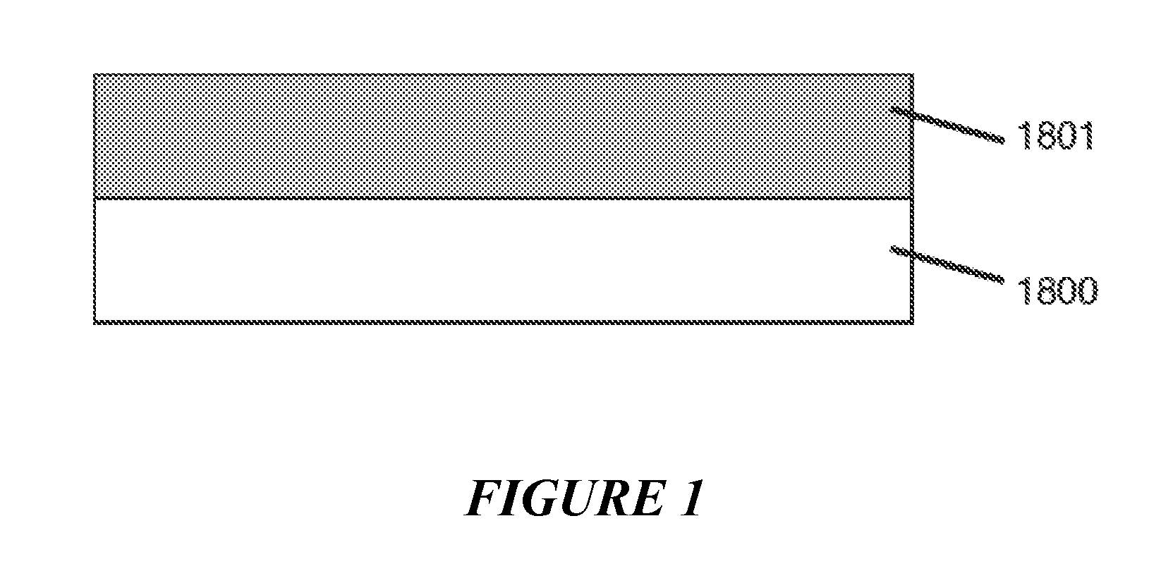
[0150]Thick, monocrystalline ZrB2 layers (up to 500 nm thick) were grown on the Si(111) hexagonal surface at a temperature, pressure and reactant concentration of 900° C., 2-4×10⁻⁶ Torr and ˜1% Zr(BH4)4 / H2, respectively. The reaction mixture based on 4 Torr / liter of Zr(BH4)4 and a large excess of research grade H2 was prepared prior to each deposition by combining the pure compounds in a 1000 mL vacuum flask at total final pressure of 400 Torr. The flask was connected to the gas injection manifold of the deposition chamber, and the manifold was pumped to ˜10−8 Torr. A boron doped (1-10 Ω-cm), Si(111) wafer was cleaved to 1 cm2 size substrates to fit the dimensions of the sample stage. Each substrate was sonicated in methanol for 5 minutes, dried under a stream of purified N2, inserted through a load lock into the growth chamber at a base pressure of 4×10⁻¹⁰ Torr, and heated at 600° C. under UHV to remove surface contaminants until the pressure...

example 2

Structural and Morphological Characterization of Epitaxial ZrB2 Layers

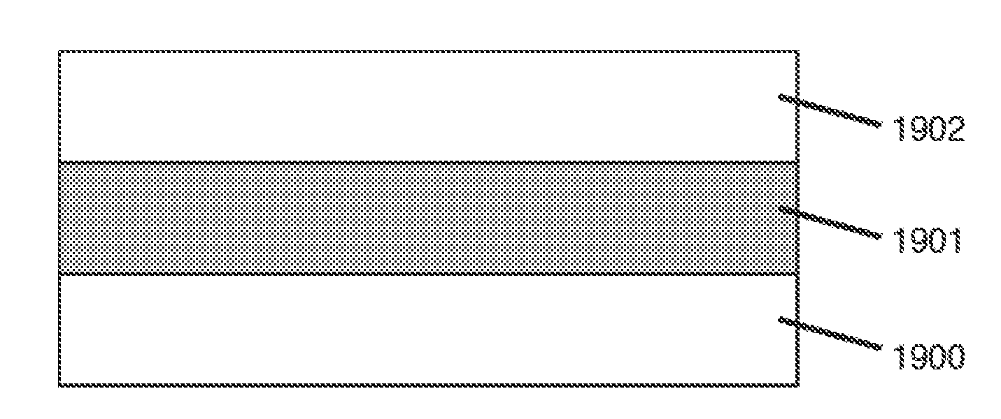
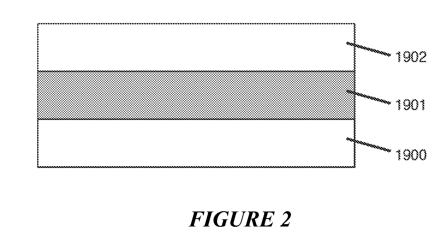
[0152]The resultant films of Example 1 are fully commensurate and perfectly oriented with the underlying hexagonal surface as evidenced by various microstructural and surface characterization techniques including Rutherford backscattering (RBS) ion channeling, atomic force microscopy (AFM) and transmission electron microscopy (XTEM) (see FIG. 3). The latter reveals that heteroepitaxy between ZrB2(0001) and Si(111) is obtained via coincidence-misfit mechanism in which five lattice rows of Si are aligned with every six rows of ZrB2, (i.e., “magic mismatch”). This registry results in a periodic array of edge dislocations along the interface which accommodate the large difference in lattice constants.

[0153]As mentioned above it is extremely critical to maintain the optimal growth conditions and any deviations, however minor, invariably result in either negligible growth of crystalline material or in the formation of p...

example 3

High Resolution XRD Film Strain Studies of Epitaxial ZrB2 Layers

[0154]The structural quality and crystallographic orientation of these thick films of Example 1 were analyzed by high resolution x-ray diffraction (HR-XRD) using a Panalytical X-pert Pro diffractometer. The θ-2θ scans revealed only the (001) and (002) peaks of the hexagonal lattice, indicating that the heterostructure is highly oriented and epitaxial. The double crystal rocking scans of ZrB2(001) showed full width at half maxima (FWHM) of 0.15 degrees for 500 nm thick films, indicating no significant tilt between the crystalline domains, consistent with extremely narrow mosaicities within the horizontal direction. For samples with a nominal thickness up to 100 nm a symmetrical envelope of interference fringes is also present in the vicinity of the ZrB2 peak in the θ-2θ diffraction patterns. For higher thickness samples these fringes merge within the parent (001) peak.

[0155]Extensive off-axis high-resolution measurements...


PUM


Abstract

Semiconductor structures are provided comprising a substrate and a epitaxial layer formed over the substrate, wherein the epitaxial layer comprises B; and one or more element selected from the group consisting of Zr, Hf and Al and has a thickness greater than 50 nm. Further, methods for integrating Group III nitrides onto a substrate comprising, forming an epitaxial buffer layer of a diboride of Zr, Hf, Al, or mixtures thereof, over a substrate; and forming a Group III nitride layer over the buffer layer, are provided which serve to thermally decouple the buffer layer from the underlying substrate, thereby greatly reducing the strain induced in the semiconductor structures upon fabrication and/or operation.

Description

CROSS-REFERENCE TO RELATED APPLICATIONS[0001]This application claims the benefit of the filing dates, under 35 USC §119(e), of U.S. Provisional Application Ser. No. 60 / 883,477, filed Jan. 4, 2007; and U.S. Provisional Application Ser. No. 60 / 973,002, filed Sep. 17, 2007, each of which are hereby incorporated by reference in their entirety.STATEMENT OF GOVERNMENT FUNDING[0002]The invention described herein was made in part with government support under grant number EEC-0438400, awarded by the National Science Foundation. The United States Government has certain rights in the invention.FIELD OF THE INVENTION[0003]The invention generally relates to the preparation and use of epitaxial buffer layers in the preparation of Group III-N materials on solid supports. In particular, the invention relates to the use of epitaxial diboride buffer layers on semiconductor substrates for use in the preparation of Group III-N overlayers.BACKGROUND OF THE INVENTION[0004]Group III nitride materials inc...

Claims


Application Information

Patent Timeline
IPC IPC(8): H01L21/36H01L29/06
CPCC30B25/183C30B29/403H01L21/0237H01L21/02381H01L21/02433H01L33/007H01L21/02502H01L21/0254H01L21/0262H01L29/24H01L21/02488H01L21/20
Inventor KOUVETAKIS, JOHNROUCKA, RADEK
Owner ARIZONA STATE UNIVERSITY
Why Eureka
Try Eureka