Methods for fabricating silicon carriers with conductive through-vias with low stress and low defect density

a technology of conductive through-vias and silicon carriers, which is applied in the direction of semiconductor devices, semiconductor/solid-state device details, electrical apparatus, etc., can solve the problems of high fabrication cost, inability or desire to use carrier technologies, and inability to achieve practical integration or chip-level integration. , to achieve the effect of low stress, high yield and high density

Inactive Publication Date: 2008-07-10
GLOBALFOUNDRIES US INC
View PDF35 Cites 133 Cited by
  • Summary
  • Abstract
  • Description
  • Claims
  • Application Information

AI Technical Summary

Benefits of technology

[0011]Exemplary embodiments of the invention generally includes to methods for fabricating silicon carrier structures with conductive through-via structures, which allow for high-density packaging of multiple integrated circuit chips. More specifically, exemplary embodiments of the invention include methods for fabricating silicon carriers with high-aspect ratio conductive through-v

Problems solved by technology

With SoC designs, the functionality of a complete system (e.g., computer) is integrated on a single silicon die, SoC solutions may not be practical or achievable for chip-level integration when a given system design requires the use of heterogeneous semiconductor technologies to fabricate the necessary system integrated circuits.
There are disadvantages associated with organic and ceramic carrier technologies including, for example, high fabrication costs and inherent limitations the practical integration, density, I/O density, power density, etc, that may be achieved using organic or ceramic carriers, as is known in the art.
It is believed that inherent limitations and high fabrication costs associated with ceramic and organic carrier technologies may limit the ability or desire to use such carrier technologies to meet the increasing demands for higher density and higher performance packaging solutions.
The ability to fabricate silicon carriers with high yield and low defect density can be problematic using conventional methods depending on, e.g., the size and geometry of the target vias (aspect ratio, width, pitch), the types of materials and/or processes used to line and

Method used


Image

  • Methods for fabricating silicon carriers with conductive through-vias with low stress and low defect density
  • Methods for fabricating silicon carriers with conductive through-vias with low stress and low defect density
  • Methods for fabricating silicon carriers with conductive through-vias with low stress and low defect density

Examples


Embodiment Construction

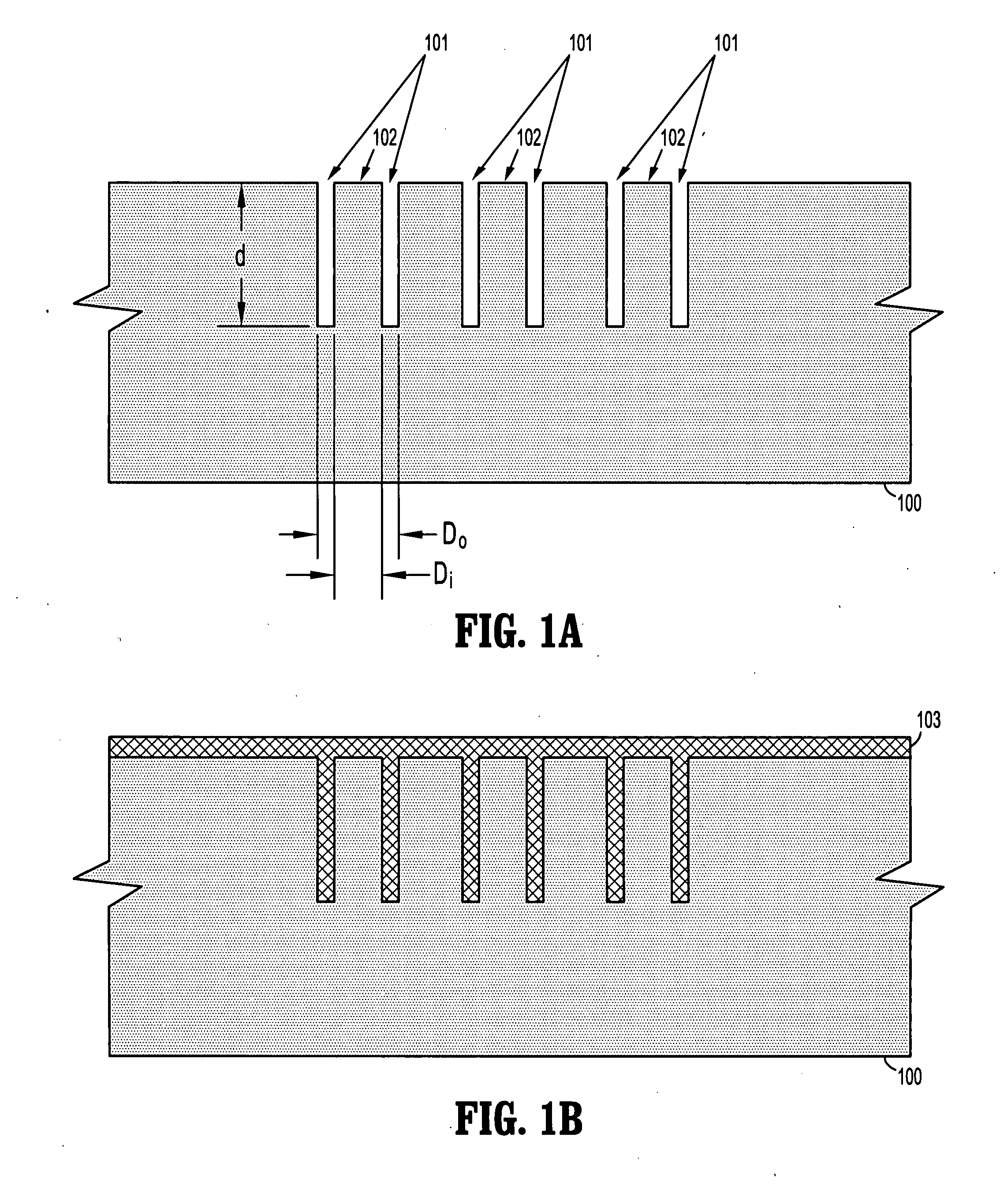
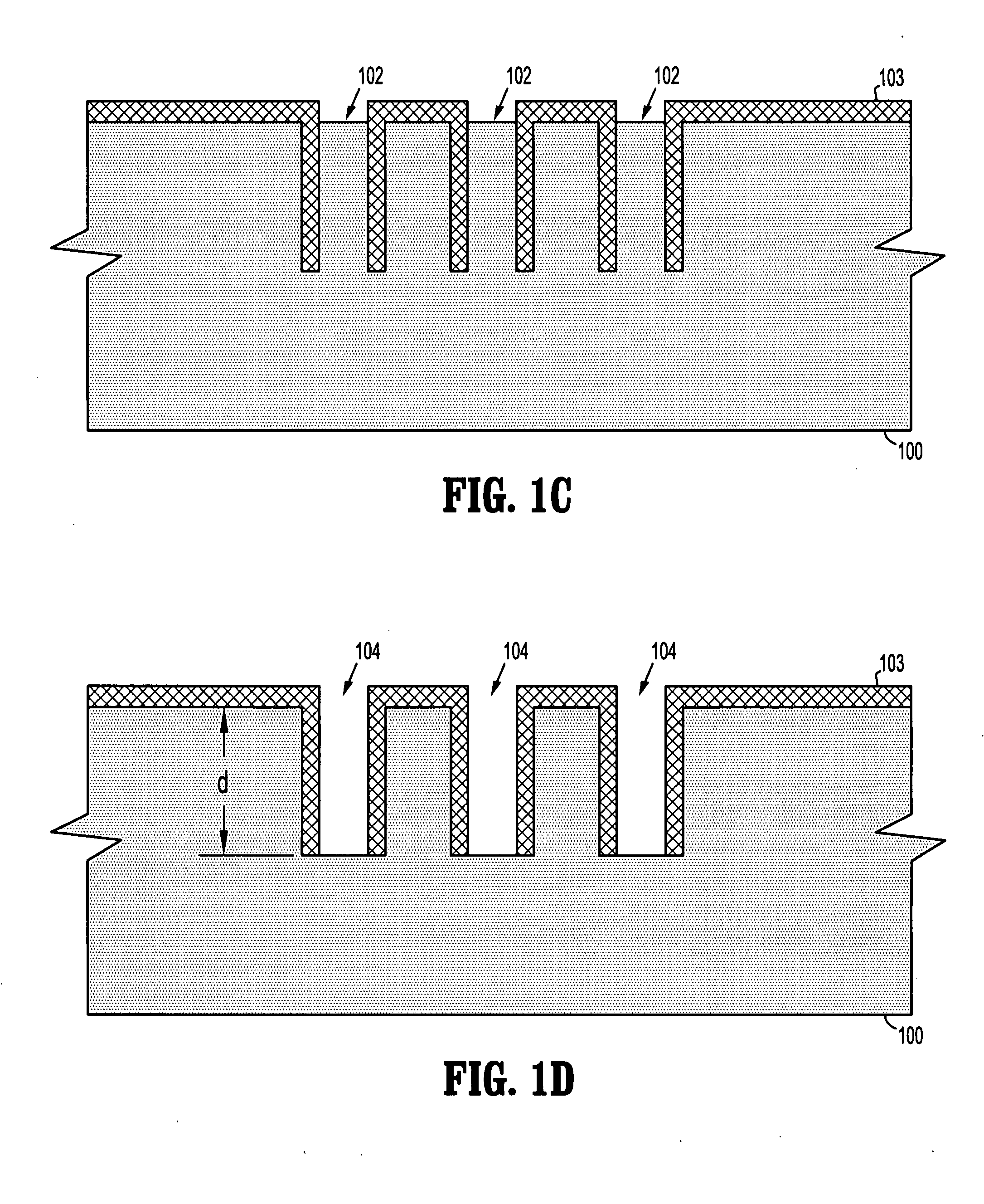
[0033]Exemplary embodiments of the invention will now be described more fully with reference to the accompanying drawings in which it is to be understood that the thickness and dimensions of the layers and regions are exaggerated for clarity. It is to be further understood that when a layer is described as being “on” or “over” another layer or substrate, such layer may be directly on the other layer or substrate, or intervening layers may also be present. Moreover, similar reference numerals used throughout the drawings denote elements having the same or similar functions.

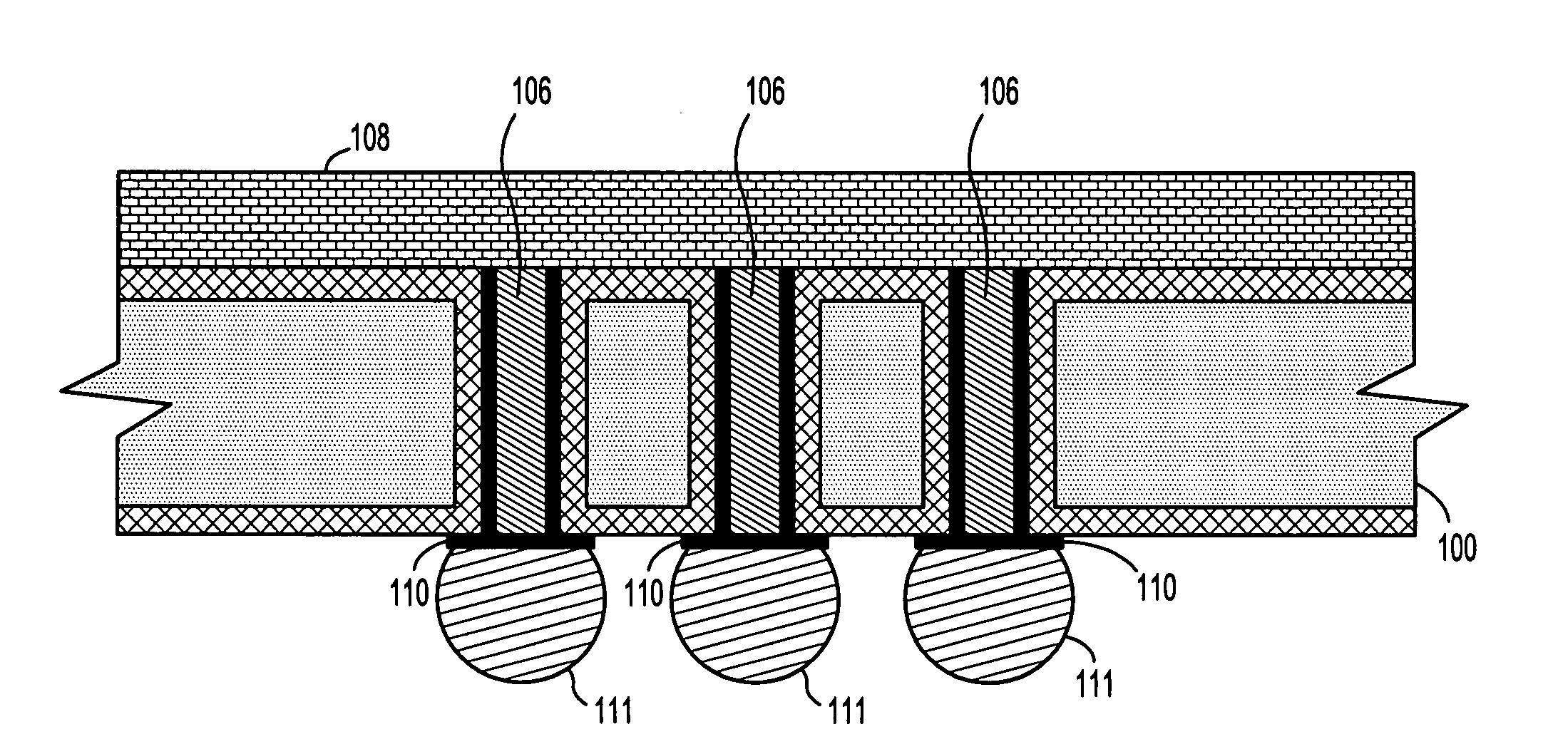
[0034]FIG. 7 is a schematic side-view of an electronic package (10) having a silicon carrier with conductive through-vias fabricated using one of various exemplary methods described herein. The electronic package (10) generally comprises an SOP (system on package) module (20) electrically and mechanically mounted to an electric circuit board (30). The SOP module (20) generally comprises a chip-level package (40) an...


PUM


Abstract

Methods are provided for fabricating silicon carriers with conductive through-vias that allow high-yield manufacture of silicon carrier with, low defect density. In particular, methods are provided which enable fabrication of silicon, carries with via diameters such as 1 to 10 microns in diameter for a vertical thickness of less than 10 micrometers to greater than 300 micrometers, which are capable robust to thermal-mechanical stresses during production to significantly minimize the thermal mechanical movement at the via sidewall interface between the silicon, insulator, liner and conductor materials.

Description

GOVERNMENT LICENSE RIGHTS[0001]This invention was made with Government support under Contract No. NBCH3039004 awarded by the Defense Advanced Research Projects Agency (aABPA) and H98230-04-C-0920 awarded by the Maryland Procurement Office. The Government has certain, rights in this invention.TECHNICAL FIELD OF THE INVENTION [0002]The present invention generally relates to silicon carrier structures for high-density packaging of multiple integrated circuit chips. More specifically, the present invention relates to methods for fabricating silicon carriers with high-aspect ratio conductive through-vias having robust structures capable of withstanding thermal-mechanical stresses encountered during fabrication, thereby allowing high-yield manufacture of silicon carriers with low stress ana low defect density.BACKGROUND [0003]Advances in semiconductor chip fabrication and packaging technologies have enabled the development of highly integrated semiconductor chips and compact chip package ...

Claims


Application Information

Patent Timeline
IPC IPC(8): H01L21/768H01L23/522
CPCH01L21/486H01L2224/16225H01L21/76898H01L23/055H01L23/433H01L23/481H01L25/0655H01L2224/73253H01L2924/01077H01L2924/01078H01L2924/01079H01L2924/04941H01L2924/12044H01L2924/15311H01L2924/16195H01L2924/3025H01L2224/16227H01L2924/10253H01L21/6835H01L2924/00
Inventor BASKER, VEERARAGHAVEN S.COTTE, JOHN MICHAELDELIGIANNI, HARIKLIAKNICKERBOCKER, JOHN ULRICHKWIETNIAK, KEITH T.
Owner GLOBALFOUNDRIES US INC
Why Eureka
Try Eureka