Programmable resistor, switch or vertical memory cell

a vertical memory cell and resistor technology, applied in the field of field programmable resistors or switches, can solve the problems of increasing the resistance of dynamic increasing the vulnerability of static random access memory arrays to soft errors, and requiring a significant amount of power for operation, so as to increase reduce the resistivity and hence the resistance of the dielectric material, and high diffusivity to copper

Inactive Publication Date: 2008-07-24
INFINEON TECH AG +1
View PDF29 Cites 71 Cited by
  • Summary
  • Abstract
  • Description
  • Claims
  • Application Information

AI Technical Summary

Benefits of technology

[0006]In view of the foregoing, disclosed herein are embodiments of a device and a method of forming the device that utilize metal ion migration (e.g., copper (Cu) ion migration) under controllable conditions to form a programmable resistor or switch. Specifically, the embodiments of the device comprise two metal electrodes (e.g., Cu electrodes) separated by one or more different dielectric materials (e.g., a low-k dielectric material with relatively high diffusivity to copper). One electrode is sealed from the dielectric material, the other is not. The device is adapted to allow controlled migration of embedded metal ions from the unsealed electrode into dielectric material to form a more conductive path with the accumulation of metal ions in dielectric under field between the electrodes in a matter of nanoseconds and, thereby, to decrease the resistivity and hence the resistance of the dielectric material. Reversing the field causes the metal ions to reverse their migration, to break the conductive path between the electrodes, and, thereby, to increase the resistance of the dielectric material. Thus, the device can comprise a simple switch or programmable resistor. Additionally, by monitoring the resistance change, a two-state, two-terminal, silicon technology-compatible, flash memory device with a very simple tuning process can be created.
[0007]More particularly, an embodiment of the device can comprise an isolation layer having a first side and a second side. A cell, such as a via, can extend through the isolation layer from the first side to the second side. This cell or via can be filled with a bulk low-k dielectric material or, alternatively, can be filled with multiple layers of at least two different low-k dielectric materials extending vertically between the first side and the second side. The material that forms the isolation layer and the dielectric fill material(s) within the cell can comprise different materials. For example, the dielectric fill material(s) within the cell can comprise low-k dielectric material(s) that have a relatively high copper ion diffusivity. Whereas, the isolation layer can comprise a material that has a relatively low copper ion diffusivity and that adheres well to low-k dielectrics. Optionally, the sidewalls of the cell can be lined with a material that provides a diffusion barrier and that further enhances adhesion of the dielectric fill material(s) within the cell. Lining the cell sidewalls, further allows the isolation layer to be formed using a conventional inter-layer dielectric (e.g., silicon dioxide (SiO2), which generally also allows for fast diffusion of copper ions). Lining the cell, also allows the same dielectric material to be used in both the isolation layer and the cell without risking copper diffusion into the isolation layer.
[0008]The device can further comprise a first metal layer (e.g., a metal electrode, such as a copper electrode) adjacent to the cell on the first side. The interface between the first metal layer and the dielectric fill material(s) is permeable to copper ions (i.e., unsealed). That is, there is no liner between the first metal layer and dielectric material or there is a liner that is sufficiently thin and / or porous to allow for metal ion diffusion from the first metal layer into the dielectric fill material(s) under certain applied electric field. Additionally, the surface of the first metal layer at this interface can be oxidized to allow for easier copper ion generation under an electric field.

Problems solved by technology

Current floating-gate flash memories are proving especially difficult to scale.
Static random access memory (SRAM) arrays are looking increasingly vulnerable to soft errors, and dynamic random access memory (DRAM) arrays are slow and require a significant amount of power for operation.
However, PCEs are not field programmable as they require a special tuning process in which electrical impulses must be applied to the phase change materials in order to “program” them to exhibit the desired resistive properties to store data.
Additionally, the integration of PCE memory with existing silicon-based integrated circuits and the high current / voltage operation mode pose concerns for real-world PCE memory applications.
Furthermore, the device is formed such that the interface between the additional metal layer above the cell and the dielectric fill material(s) within the cell is sealed and will not allow migration of metal ions into the cell.
Thus, in this embodiment the device is formed such that the interface between the metal layer below the cell and the dielectric fill material(s) within the cell is sealed and will not allow migration of metal ions into the cell.

Method used


Image

  • Programmable resistor, switch or vertical memory cell
  • Programmable resistor, switch or vertical memory cell
  • Programmable resistor, switch or vertical memory cell

Examples


Embodiment Construction

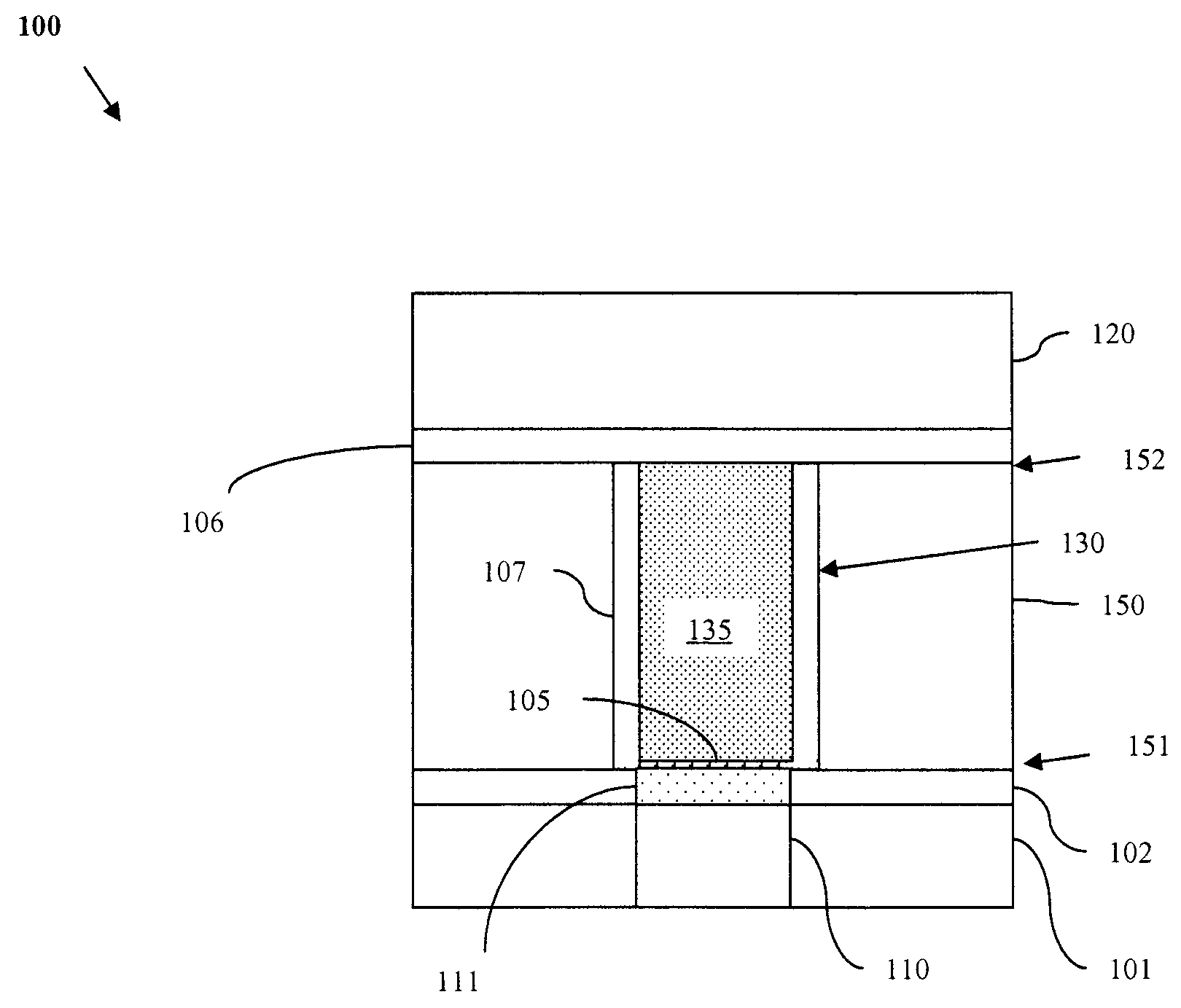
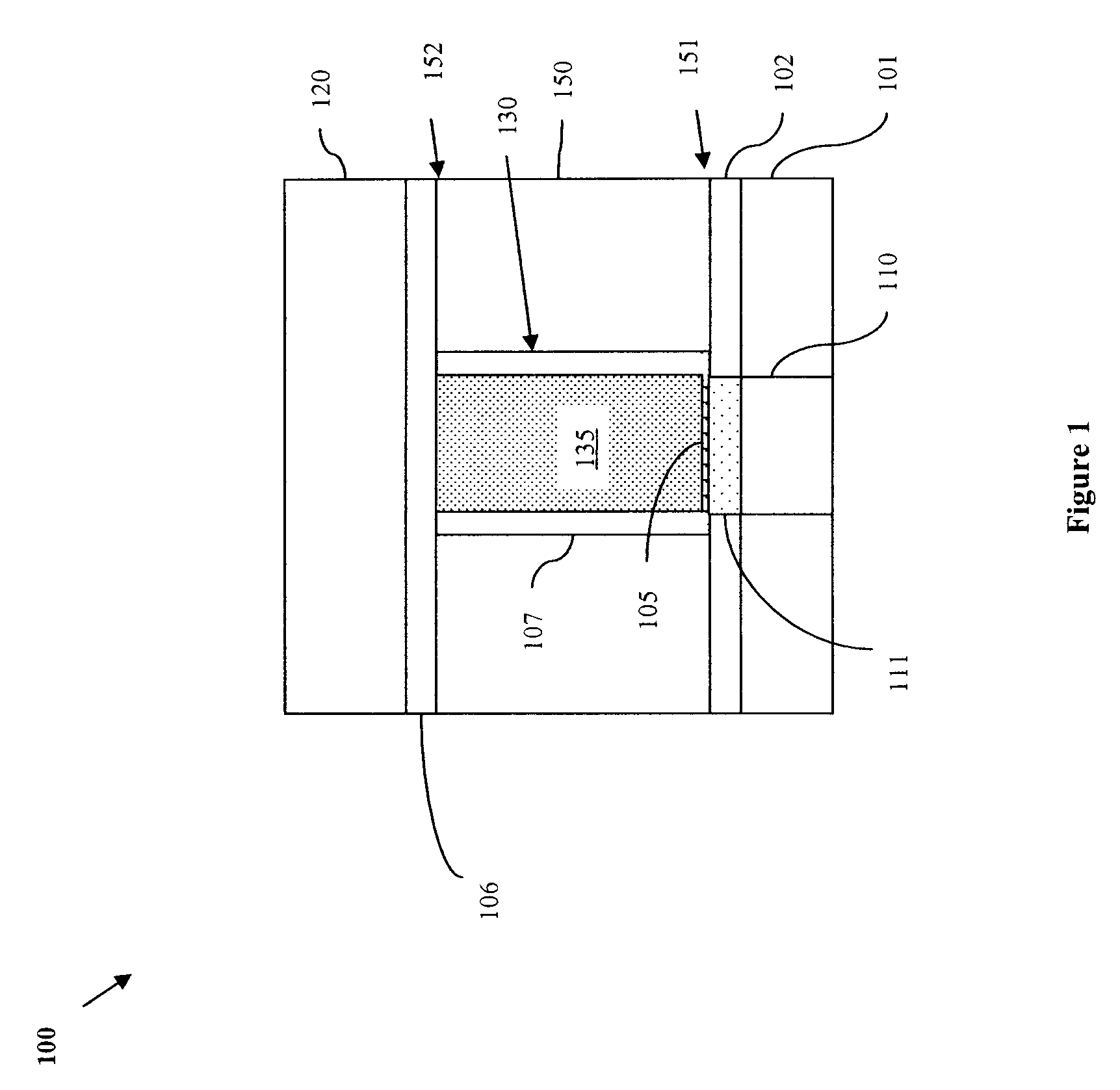
[0057]The embodiments of the invention and the various features and advantageous details thereof are explained more fully with reference to the non-limiting embodiments that are illustrated in the accompanying drawings and detailed in the following description. It should be noted that the features illustrated in the drawings are not necessarily drawn to scale. Descriptions of well-known components and processing techniques are omitted so as to not unnecessarily obscure the embodiments of the invention. The examples used herein are intended merely to facilitate an understanding of ways in which the embodiments of the invention may be practiced and to further enable those of skill in the art to practice the embodiments of the invention. Accordingly, the examples should not be construed as limiting the scope of the embodiments of the invention.

[0058]As mentioned above, there is a need in the art for a device (e.g., a programmable resistor) that is both field programmable and can be inc...


PUM

PropertyMeasurementUnit
voltageaaaaaaaaaa
timeaaaaaaaaaa
on-timeaaaaaaaaaa

Abstract

Disclosed are embodiments of a device and method of forming the device that utilize metal ion migration under controllable conditions. The device embodiments comprise two metal electrodes separated by one or more different dielectric materials. One electrode is sealed from the dielectric material, the other is not. The device is adapted to allow controlled migration of embedded metal ions from the unsealed electrode into dielectric material to form a conductive path under field between the electrodes and, thereby, to decrease the resistance of the dielectric material. Reversing the field causes the metal ions to reverse their migration, to break the conductive metallic path between the electrodes and, thereby, to increase the resistance of the dielectric material. Thus, the device can comprise a simple switch or programmable resistor. Additionally, by monitoring the resistance change, a two-state, two-terminal, silicon technology-compatible, flash memory device with a very simple tuning process can be created.

Description

BACKGROUND[0001]1. Field of the Invention[0002]The embodiments of the invention generally relate to programmable resistors, and, more particularly, to a field programmable resistor or switch that can be incorporated into a memory array as a memory cell.[0003]2. Description of the Related Art[0004]Existing limitations of current memory technologies represent opportunities for alternatives. Current floating-gate flash memories are proving especially difficult to scale. Static random access memory (SRAM) arrays are looking increasingly vulnerable to soft errors, and dynamic random access memory (DRAM) arrays are slow and require a significant amount of power for operation. Phase change random access memory (PCRAM) arrays are an emerging non-volatile memory technology, which attempts to overcome the limitations of SRAM and DRAM arrays. This PCRAM technology is based on a structure called a phase change element (PCE), which is generally understood to be a programmable resistor. For examp...

Claims


Application Information

Patent Timeline
Patent Type & Authority Applications(United States)
IPC IPC(8): H01L29/00H01L21/02
CPCH01L27/2463H01L45/085H01L45/1233H01L45/1683H01L45/14H01L45/145H01L45/1616H01L45/1266H10B63/80H10N70/245H10N70/8416H10N70/881H10N70/883H10N70/023H10N70/826H10N70/066
Inventor CHEN, FENFISCHER, ARMINGILL, JASON P.
Owner INFINEON TECH AG
Why Eureka
Try Eureka