Layered amorphous diamond materials and associated methods for enhanced diamond electroluminescence
a diamond and amorphous technology, applied in the manufacture of electrode systems, electric discharge tubes/lamps, discharge tubes luminescence screens, etc., can solve the problems of limiting the potential use limiting the range of applications, and limiting the efficiency of field emission devices, so as to enhance the overall luminescence intensity of the device, enhance the overall luminescence intensity, and enhance the effect of luminescence intensity
- Summary
- Abstract
- Description
- Claims
- Application Information
AI Technical Summary
Benefits of technology
Problems solved by technology
Method used
Image
Examples
example 1
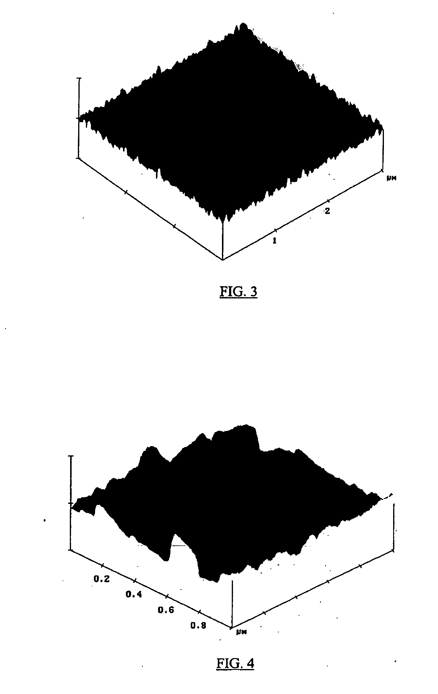
[0115]An amorphous diamond material was made as shown in FIG. 3, using cathodic arc deposition. Notably, the asperity of the emission surface has a height of about 200 nanometers, and a peak density of about 1 billion peaks per square centimeter. In the fabrication of such material, first, a silicon substrate of N-type wafer with (200) orientation was etched by Ar ions for about 20 minutes. Next, the etched silicon wafer was coated with amorphous diamond using a Tetrabond® coating system made by Multi-Arc, Rockaway, N.J. The graphite electrode of the coating system was vaporized to form an electrical arc with a current of 80 amps, and the arc was drive by a negative bias of 20 volts toward the silicon substrate, and deposited thereon. The resulting amorphous diamond material was removed from the coating system and observed under an atomic force microscope, as shown in FIGS. 3 and 4.
[0116]The amorphous diamond material was then coupled to an electrode to form a cathode, and an electr...
example 2
[0117]A 10 micron layer of copper can be deposited on a substrate using sputtering. Onto the copper was deposited 2 microns of samarium by sputtering onto the copper surface under vacuum. Of course, care should be taken so as to not expose the beryllium to oxidizing atmosphere (e.g. the entire process can be performed under a vacuum). A layer of amorphous diamond material can then be deposited using the cathodic arc technique as in Example 1 resulting in a thickness of about 0.5 microns. Onto the growth surface of the amorphous diamond a layer of magnesium can be deposited by sputtering, resulting in a thickness of about 10 microns. Finally a 10 microns thick layer of copper was deposited by sputtering to form the anode.
example 3
[0118]A 10 micron layer of copper can be deposited on a substrate using sputtering. Onto the copper was deposited 2 microns of cesium by sputtering onto the copper surface under vacuum. Of course, care should be taken so as to not expose the cesium to oxidizing atmosphere (e.g. the entire process can be performed under a vacuum). A layer of amorphous diamond material can then be deposited using the cathodic arc technique as in Example 1 resulting in a thickness of about 65 nm. Onto the growth surface of the amorphous diamond a layer of molybdenum can be deposited by sputtering, resulting in a thickness of about 16 nm. Additionally, a 20 nm thick layer of In-Sn oxide was deposited by sputtering to form the anode. Finally, a 10 micron layer of copper was deposited on the In-Sn layer by sputtering. The cross-sectional composition of the assembled layers is shown in part by FIG. 9A as deposited. The assembled layers were then heated to 400° C. in a vacuum furnace. The cross-sectional co...
PUM
 Abstract
Description
Claims
Application Information


