Quartz component for plasma processing apparatus and restoring method thereof

a plasma processing apparatus and component technology, applied in the field of plasma processing technique, can solve the problems of plasma damage, damage to components, and inability to completely eliminate the problem of plasma damage, so as to reduce the running cost of the plasma processing apparatus and improve the efficiency of resource utilization

Inactive Publication Date: 2008-08-28
KAWASAKI MICROELECTRONICS
View PDF24 Cites 7 Cited by
  • Summary
  • Abstract
  • Description
  • Claims
  • Application Information

AI Technical Summary

Benefits of technology

[0013]This invention has been made, according to various exemplary embodiments, in order to address the above-described problems, and accordingly, this invention provides a quartz component for a plasma processing apparatus, and a restoring method which enables restoration of the chamber components, and in particular, that enables repeated use of the component without adversely influencing the plasma process.
[0019]Thus, use of the component over a long period of time is enabled by repeating the restoration process of the component damaged due to its use within the plasma processing apparatus, thereby reducing the running costs of the plasma processing apparatus, and improving the efficiency of utilization of resources.

Problems solved by technology

In dry etching techniques, however, components within the chamber of a plasma processing apparatus are often damaged due to their exposure to the plasma.
In particular, a dry etching apparatus for etching silicon oxide, which requires high-energy ions, presents a serious problem in that it damages the components.
However, none of the aforementioned materials can completely eliminate the problem of plasma damage.
In the event that the user uses a plasma processing apparatus, including the chamber components, beyond their predetermined duration of use, the damaged components may create a problem of, for example, unstable plasma discharge.
When the plasma damages any of chamber components, new current paths are formed, leading to the problem that a desired plasma discharge cannot be sustained.
Furthermore, the flow of reactive gas may be influenced due to the damage of the chamber components, and unwanted particles may be generated from the damaged components.
Accordingly, replacement of the entire chamber component leads to unnecessarily high costs, and to waste of resources.
However, dividing a single component into multiple sub-components increases the number of chamber components, and leads to a problem of increased management costs.

Method used


Image

  • Quartz component for plasma processing apparatus and restoring method thereof
  • Quartz component for plasma processing apparatus and restoring method thereof
  • Quartz component for plasma processing apparatus and restoring method thereof

Examples


first embodiment

[0033]Description will be made below regarding a first exemplary embodiment according to this invention.

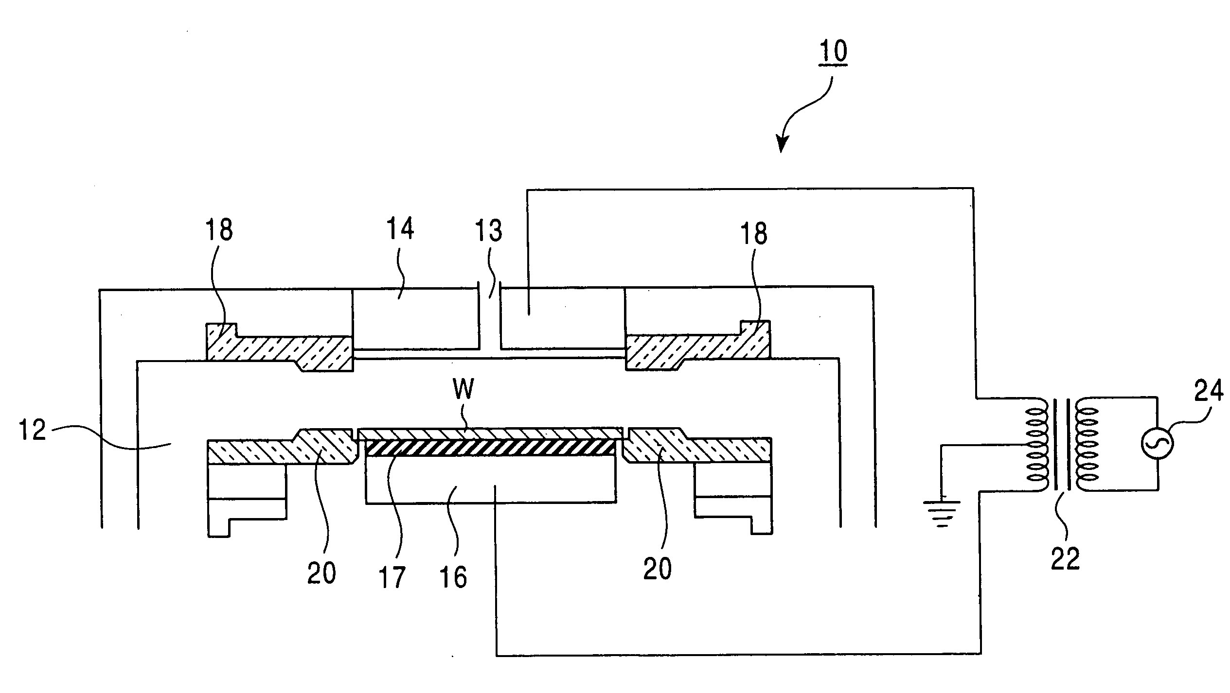
[0034]FIG. 1 is a schematic cross-sectional diagram of a plasma processing apparatus for performing dry etching according to an exemplary embodiment of this invention. As shown in FIG. 1, the plasma processing apparatus 10 performs etching using radio-frequency (RF) plasma. The plasma processing apparatus 10 has a parallel-plate-electrode configuration with the electrodes facing one another across a narrow gap.

[0035]The processing chamber 12 accommodates a silicon wafer W to be processed, and a vacuum of around 10−6 Torr (10−4 Pa) can be established. The chamber 12 includes an upper electrode 14 at the upper middle thereof and a lower electrode 16 at the lower middle thereof. The upper electrode 14 is connected to a gas inlet 13 for introducing the etching gas. The lower electrode 16 has an electrostatic chuck 17 for mounting the wafer W which is to be etched.

[0036]The side surfac...

second embodiment

[0115]Next, description will be made regarding a method for performing a cycle of use and restoration of a quartz component according to various exemplary embodiments of this invention.

[0116]FIG. 6 is a flowchart that shows a flow of a cycle of use and restoration according to various exemplary embodiments of this invention, and FIGS. 7 and 8 are longitudinal cross-sectional diagrams of a quartz component that is used during the cycle of use and restoration according to various exemplary embodiments.

[0117]According to various exemplary embodiments, the first time, a conventional focus ring having a generally flat upper surface (main surface) is used. After processing a number of wafers W, a first time restoration is performed on the focus ring such that the upper surface becomes flat for its use a second time.

[0118]After processing a number of wafers W, a second restoration is performed. This time, restoration is performed so that the focus ring is formed with a configuration where ...

example

[0154]Description will be made below with reference to the drawings regarding the operation of an exemplary plasma processing apparatus according to this invention. The same plasma processing apparatus as shown in FIG. 1 is used.

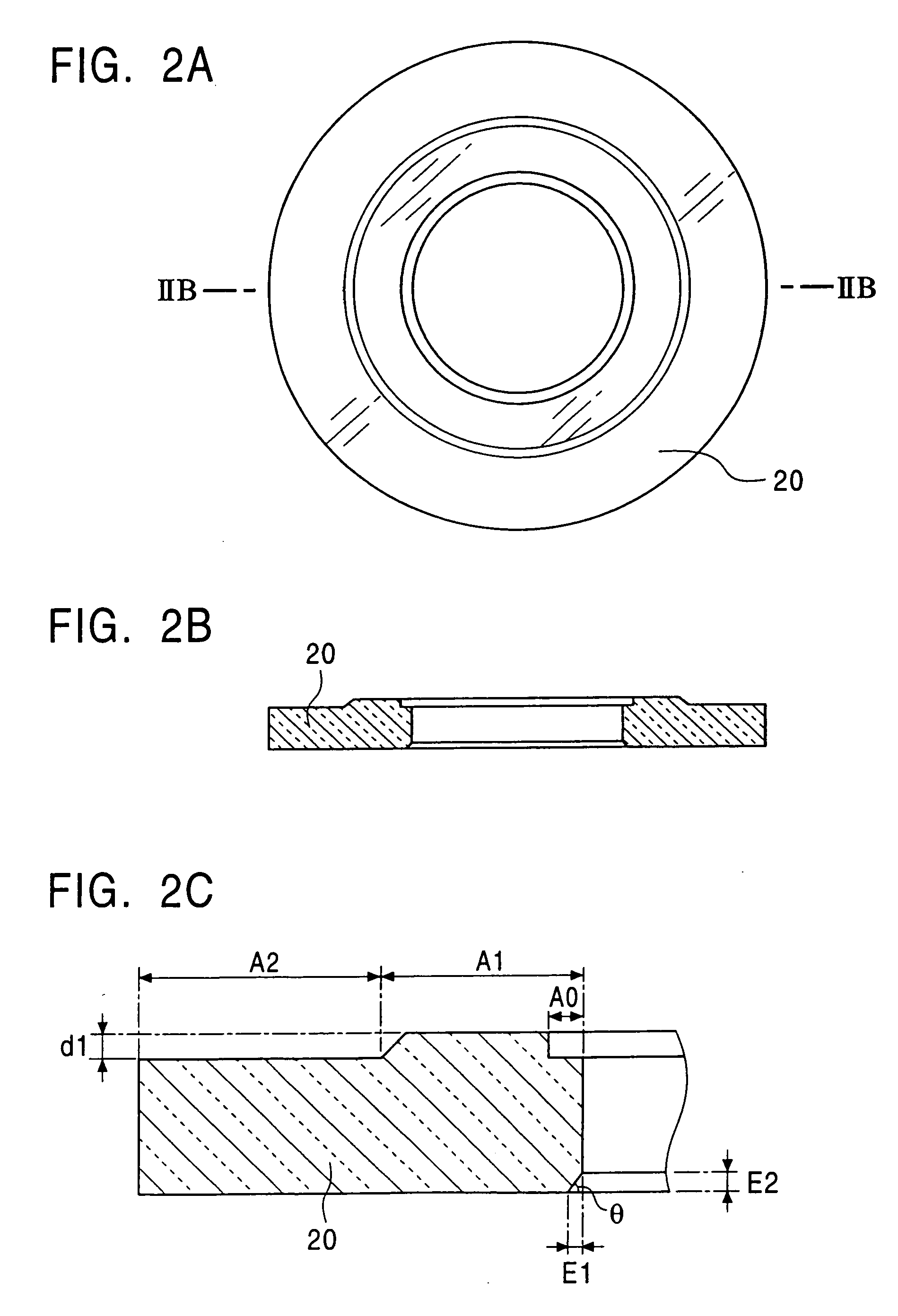
[0155]In this example, split-coupling method for applying RF electric power to both the upper and lower electrodes was employed. In this example, as shown in FIGS. 2 and 3, quartz components (focus ring and shield ring), each having a main surface with a ridge in the shape of a circle are used.

[0156]The first region, or the ridged region, was formed with a width of 35 mm around the inner perimeter, and the main surface was divided into the first region and the second region separated in height by an offset with a height of 1 mm. Furthermore, a beveled portion of 2R is formed on the inner perimeter of the mounting surface (lower face) of the focus ring. Dry etching is performed for a silicon-dioxide film using the plasma processing apparatus 10 shown in FIG. ...


PUM

PropertyMeasurementUnit
heightaaaaaaaaaa
heightaaaaaaaaaa
heightaaaaaaaaaa

Abstract

The main surface of a quartz component is divided by an offset into a first region having a larger height around an inner perimeter and a second region adjacent to the outer perimeter of the first region. Repeated restoration of a damaged component by forming a bulge on the first region and machining the bulge to make a flat surface while maintaining the offset enables long term use of the component.

Description

[0001]This is a Division of application Ser. No. 10 / 790,188 filed Mar. 2, 2004. The disclosure of the prior application is hereby incorporated by reference herein in its entirety. This invention was first described in Japanese Patent Application No. 2003-55620, which is hereby incorporated by reference in its entirety.BACKGROUND OF THE INVENTION[0002]1. Field of Invention[0003]This invention relates to a plasma processing technique for manufacturing semiconductor devices, and particularly to a quartz component employed in plasma processing apparatus. This invention also relates to a method for restoring the quartz component.[0004]2. Description of Related Art[0005]Plasma processes, such as dry etching, are widely employed in manufacturing semiconductor devices. For example, etching is generally performed using a reactive gas activated by plasma. In dry etching techniques, however, components within the chamber of a plasma processing apparatus are often damaged due to their exposure ...

Claims


Application Information

Patent Timeline
Patent Type & Authority Applications(United States)
IPC IPC(8): B32B43/00H01J37/32H01L21/00H01L21/3065H01L21/683
CPCH01L21/67069H01J37/32623Y10S438/905
Inventor SUZUKI, KATSUNORINAKAMURA, KENJI
Owner KAWASAKI MICROELECTRONICS
Why Eureka
Try Eureka