Manufacturing method for display device

a display device and manufacturing method technology, applied in the field of insulatedgate field effect transistors, can solve the problems of increasing the size and cost of the whole processing system, the need for evacuation systems, and the space for installing evacuation systems, so as to reduce the size of the manufacturing plant and the machine, and simplify the process steps.

Inactive Publication Date: 2008-08-28
SEMICON ENERGY LAB CO LTD
View PDF72 Cites 35 Cited by
  • Summary
  • Abstract
  • Description
  • Claims
  • Application Information

AI Technical Summary

Benefits of technology

[0014]By fabricating a display device using the liquid drop ejector having the liquid drop irradiation head on which dotlike liquid drop ejection holes are arranged, the liquid drop ejector having the liquid drop ejection head on which dotlike liquid drop ejection holes are linearly arranged, and the plasma processing apparatus having plasma generation means under atmospheric condition, a waste of the material (the material of interconnects and the like in the liquid drop ejection method and gases in the case of a plasma) can be reduced. At the same time, the manufacturing cost can be reduced. In addition, by using the aforementioned apparatus simplifying the process steps, miniaturizing, reducing in size of manufacturing plant, and machines. In consequence, the fabrication plant can be reduced in size. Also, Shortening can be accomplished. In addition, the equipment of evacuation system that has been required heretofore can be simplified. In this way, the energy can be reduced. Hence, the environmental load can be reduced. Investment costs such as equipment costs have been reduced greatly.
[0015]In addition, the invention provides a fabrication process corresponding to large-sized substrates, and solves various problems such as growth in size of equipment and increase in the processing time arising from growth in size of conventional equipment.

Problems solved by technology

To attach these equipments, the cost of the evacuation system and the space for installing the evacuation system are necessary in addition to the processing apparatus.
Therefore, the size and cost of the whole processing system are increased.

Method used


Image

  • Manufacturing method for display device
  • Manufacturing method for display device
  • Manufacturing method for display device

Examples


embodiment mode 1

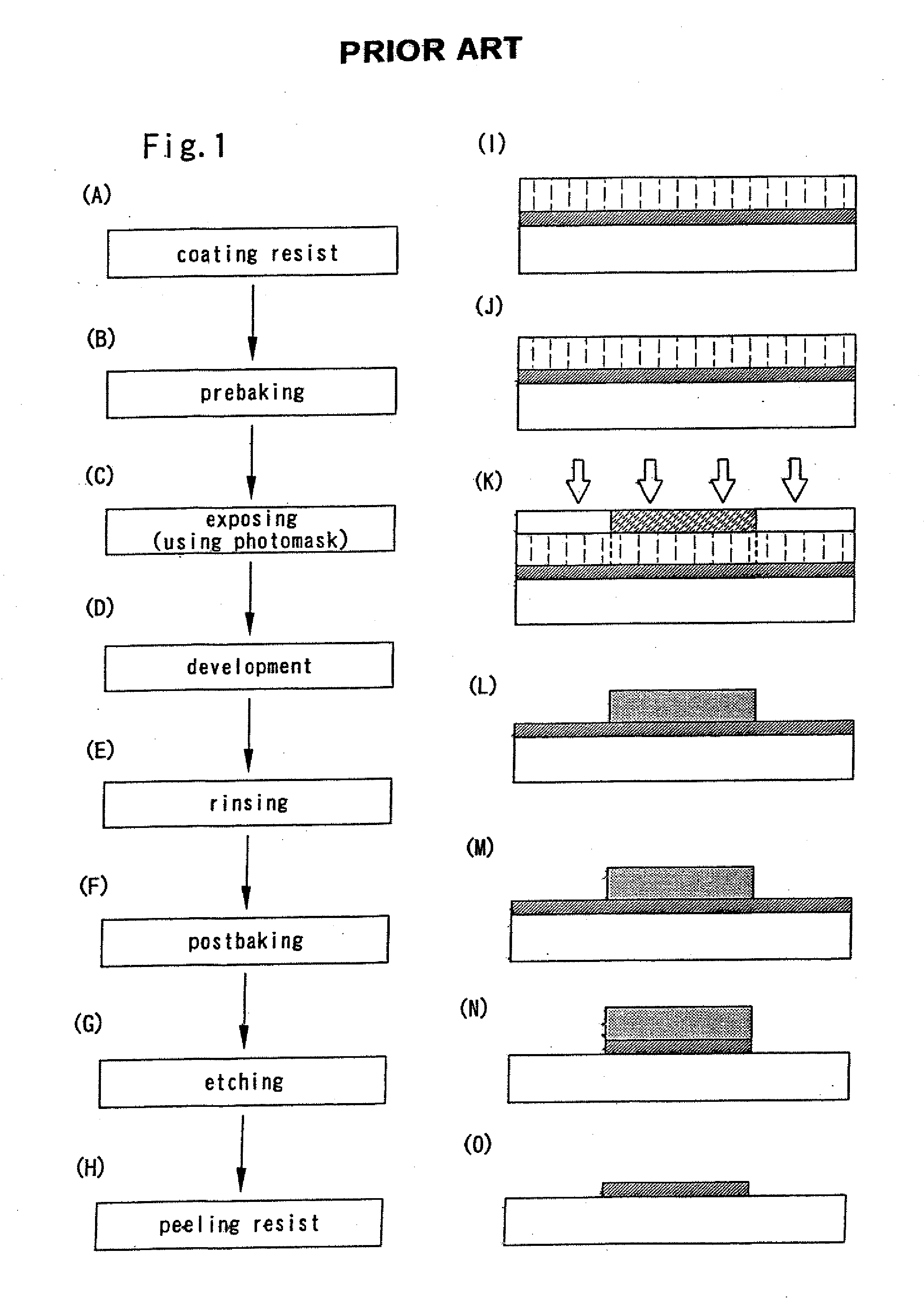
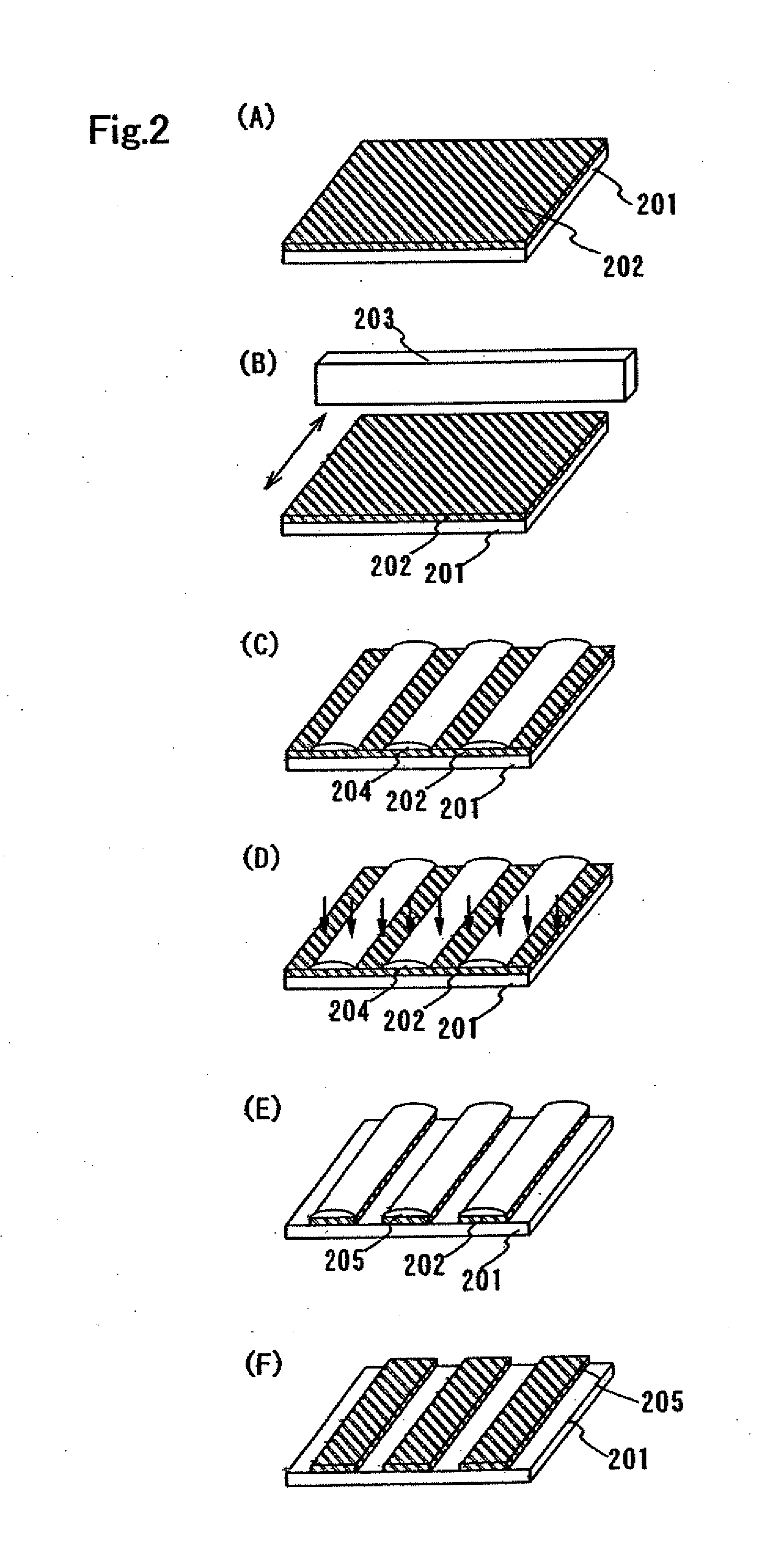
[0033]In an Embodiment mode of the invention, an wiring pattern of a semiconductor device on a glass substrate of a desired size is formed by using liquid drop ejectors and a plasma processing apparatus having a plasma generation means at or near atmospheric pressure. The invention is especially intended for application to a substrate of increasing in size such as of the fifth generation (e.g., 1000×1200 mm or 1100×1250 mm) or of the sixth generation (e.g., 1500×1800 mm). Embodiment mode 1 of the invention is hereinafter described with reference to FIG. 2 that is an accompanying drawing.

[0034]Note that the expression “liquid drop ejectors” simply referred to in Embodiment mode 1 embraces both a liquid drop ejector fitted with a head having dotlike liquid drop ejection holes and a liquid drop ejector fitted with a head having liquid drop ejection holes consisting of linear arrays of dotlike ejection holes.

[0035]First, a film 202 is formed over a substrate 201 to be processed, using a...

embodiment mode 2

[0036]A liquid drop ejector having a liquid drop ejection head in which dotlike liquid drop ejection holes are arranged can be used in Embodiment Mode 1 and is hereinafter described with reference to the accompanying drawings. FIG. 3 is a schematic perspective view showing one example of configuration of the dotlike liquid drop ejector. FIG. 4 is a view showing a head portion in which nozzles are arranged and which is used in this dotlike liquid drop ejector.

[0037]The dotlike liquid drop ejector shown in FIG. 3 comprises a head 306 inside the apparatus. A desired pattern of liquid drops is obtained over a substrate 302 by ejecting liquid drops from the head 306. In the present dotlike liquid drop ejector, besides a glass substrate or the like having a desired size, a resin substrate typified by a plastic substrate or an object to be processed such as a semiconductor wafer typified by silicon can be used as the substrate 302.

[0038]In FIG. 3, the substrate 302 is transported into a ca...

embodiment mode 3

[0069]A linear liquid drop ejector that can be used in Embodiment Mode 1 is described with reference to the accompanying drawings. The present apparatus has a liquid drop ejection head in which dotlike liquid drop ejection holes are arranged linearly. FIG. 6(A) is a schematic perspective view showing one example of configuration of the linear liquid drop ejector. Also, FIG. 6(B) is a view showing a head in which nozzles used in this linear liquid drop ejector are arranged.

[0070]The linear liquid drop ejector shown in FIG. 6(A) has the head 606 in the apparatus. A desired liquid drop pattern is obtained on a substrate 602 by ejecting liquid drops thereby. In the present linear liquid drop ejector, a glass substrate of desired size can be used as the substrate 602. In addition, a resin substrate typified by a plastic substrate or a semiconductor wafer or the like typified by silicon may also be used as the substrate 602.

[0071]In FIG. 6(A), the substrate 602 is conveyed into the casing...


PUM

PropertyMeasurementUnit
sizeaaaaaaaaaa
sizeaaaaaaaaaa
sizeaaaaaaaaaa

Abstract

With an interconnected fabrication step using the prior art photolithography, major portions of resist, interconnected material, and process gas necessary during plasma processing are wasted. Furthermore, a pumping means such as a vacuum system is necessary. Therefore, the whole equipment is increased in size. Consequently, as the processed substrate is increased in size, the manufacturing cost is increased. Accordingly, a means consisting of directly spraying the resist and interconnected material as liquid drops on necessary locations over the substrate to delineate a pattern is applied. Also, a means consisting of performing a vapor-phase reaction process such as ashing or etching at or near atmospheric pressure is applied.

Description

TECHNICAL FIELD[0001]The present invention relates to an insulated-gate field-effect transistor typified by a thin-film transistor (TFT) and to a method of fabricating it.BACKGROUND ART[0002]in recent years, flat panel displays (FPDs) typified by liquid crystal displays (LCDs) and EL displays have attracted attention as display devices that replace conventional CRTs. Especially, development of a large area liquid-crystal TVs equipped with an active-matrix-driven, large-sized liquid crystal panel is an important subject on which liquid crystal panel manufacturers should concentrate their efforts.[0003]On an active-matrix-driven liquid crystal panel, thin-film transistors (TFTs) are formed as switching elements. Conventionally, film formation and lithography using vacuum processes have been used to fabricate circuit patterns of thin-film transistors and the like.[0004]Film formation is a technique for depositing a thin film after evacuating the inside of a process chamber to a subatmo...

Claims


Application Information

Patent Timeline
Patent Type & Authority Applications(United States)
IPC IPC(8): H01L33/00H05H1/24B05D5/12G02F1/1343G03F1/00H01L21/02H01L21/027H01L21/3065H01L21/77
CPCG02F1/13439G03F7/16H01L27/1292H01L21/0273G03F7/2018H01L21/0274H01L27/1214
Inventor YAMAZAKI, SHUNPEI
Owner SEMICON ENERGY LAB CO LTD
Why Eureka
Try Eureka