Method, Apparatus, Material, and System of Using a High Gain Avalanche Photodetector Transistor

a photodetector transistor and high gain technology, applied in the direction of basic electric elements, electrical equipment, semiconductor devices, etc., can solve the problems of nai detectors with relatively poor energy resolution, terrorist use of radioactive materials, and serious threat to civil and military activities, and achieve excellent snr, good relative signal, and high temporal resolution

Inactive Publication Date: 2008-09-25
SINGH RANBIR
View PDF21 Cites 20 Cited by
  • Summary
  • Abstract
  • Description
  • Claims
  • Application Information

AI Technical Summary

Benefits of technology

[0032]1. A large bandgap, to allow operation at room temperature (high temperatures), without thermally generated noise;
[0033]2. High electron and hole mobilities, and higher saturation velocities, which lead to fast signal collection;
[0035]4. A low dielectric constant, which lowers the capacitance and, therefore, the noise;
[0039]It is worth noting that Si, GaN, SiC, or another wide bandgap material offers significant advantages as a material of choice for realizing photonic detectors because: (a) the detectors offer excellent SNR (good relative signal) even at higher temperatures, because the detector diodes offer negligible leakage current, resulting from thermally generated charge carriers; and (b) Another potential advantage is its higher temporal resolution. Since it has a high breakdown field devices may be operated under a large applied electric field. Furthermore, charge carriers may move at higher saturation velocities, thus, achieving very fast output current signals.
[0040]One of the essential features of this invention is that the avalanche current of the photodetector is enhanced by the gain of the transistor, which depends on the width of the undepleted wide-base region of the transistor. This enables the photodetector to have a more uniform and reasonably low operating avalanche bias voltage, and high optical to electrical gain.
[0041]Another feature is the control of the wavelength of absorption through the control of the doping of the emitter or the top region of the structure. This allows wider applicability to various frequencies of light using the same basic structure. Therefore, it is more cost effective for production or manufacturing.

Problems solved by technology

Terrorist use of radioactive nuclear materials is a serious threat for mass destruction or disruption of civil and military activities.
Most worrisome is the use of nuclear devices that may cause massive casualties to people and damage to structures.
NaI detectors have relatively poor energy resolutions.
This limits their use in high background situations, or for unknown sources with many closely-spaced peaks.
Gamma-ray peaks from a weak source will be difficult to observe in a relatively high background environment, and peaks that differ by a few percent in energy will usually be unresolved.
Similarly, Gas-based detectors have poor resolution, and are bulky with poor vibration performance.
Ge detectors have the disadvantage that they must be operated at low temperatures (less than 100 K) to avoid electronic noise, which is an obvious and severe logistical problem.

Method used


Image

  • Method, Apparatus, Material, and System of Using a High Gain Avalanche Photodetector Transistor
  • Method, Apparatus, Material, and System of Using a High Gain Avalanche Photodetector Transistor
  • Method, Apparatus, Material, and System of Using a High Gain Avalanche Photodetector Transistor

Examples


Embodiment Construction

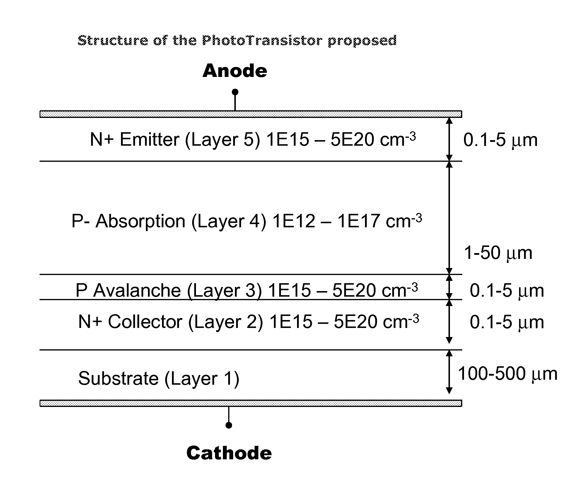
[0051]Here are some of the improvements on the design and structure:

[0052]Not only we have separated the regions as described in FIG. 5, we have used the transistor structure for higher gain, as described above. Instead, the avalanche only occurs in the multiplication region, thus, causing better uniformity for different devices. However, higher doped Multiplication region of the photodiode may not be required in the phototransistor, because multiplication is going to occur in that undepleted region of the transistor anyway. The avalanche multiplication process is further enhanced by the gain of the transistor which increases exponentially with the operating bias.

[0053]FIG. 8 indicates the Electric field corresponding to a proposed structure.

[0054]As an embodiment, only 2 terminals are electrically connected to an external biasing and / or detection circuit. The two terminals are emitter and collector (or anode and cathode).

[0055]One of the problems with semiconductor devices is the n...


PUM


Abstract

Here, we demonstrate new material / structures for the photodetectors, using semiconductor material. For example, we present the Tunable Avalanche Wide Base Transistor as a photodetector. Particularly, SiC, GaN, AlN, Si and Diamond materials are given as examples. The desired properties of an optimum photodetector is achieved. Different variations are discussed, both in terms of structure and material.

Description

BACKGROUND OF THE INVENTION[0001]Terrorist use of radioactive nuclear materials is a serious threat for mass destruction or disruption of civil and military activities. Most worrisome is the use of nuclear devices that may cause massive casualties to people and damage to structures. A device that combines radioactive materials with conventional explosives to make a radiological dispersion device is commonly called a “dirty bomb.” The procurement of nuclear materials for this purpose, the construction of the bomb, and its use are all easier than those of a nuclear weapon. Thus, it is important to detect the transport of the radiological dispersion devices and the materials needed for their construction. These materials emit gamma rays or neutrons, which can be detected to show the presence and amounts of such materials using radiation detectors.[0002]High-efficiency gamma-ray and neutron detectors are required to provide information to intercept nuclear materials and devices prior to...

Claims


Application Information

Patent Timeline
Patent Type & Authority Applications(United States)
IPC IPC(8): H01L31/107H01L27/14
CPCH01L27/1446H01L31/1105H01L31/107
Inventor SINGH, RANBIR
Owner SINGH RANBIR
Why Eureka
Try Eureka