

Method for manufacturing semiconductor device
- Summary
- Abstract
- Description
- Claims
- Application Information
AI Technical Summary
Benefits of technology
Problems solved by technology
Method used
Image

Examples
embodiment mode 1
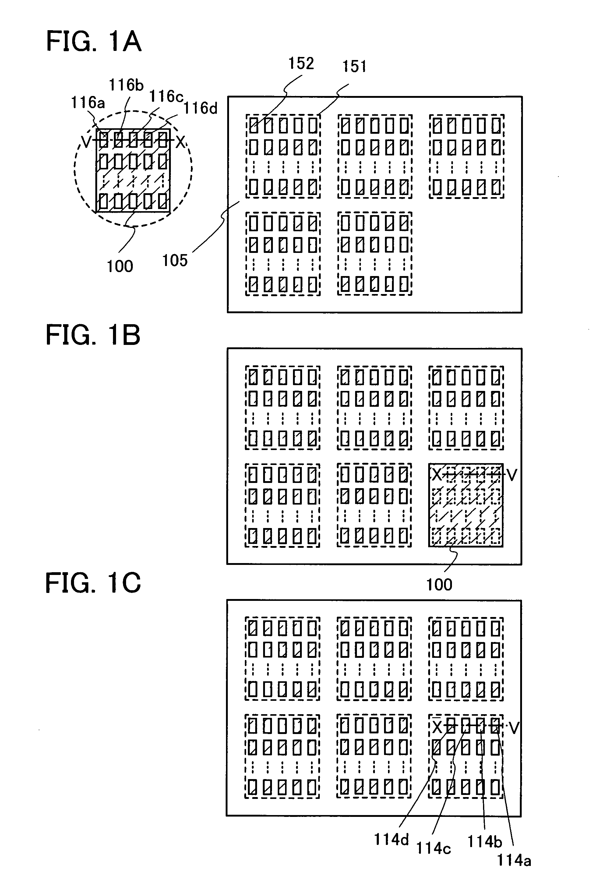
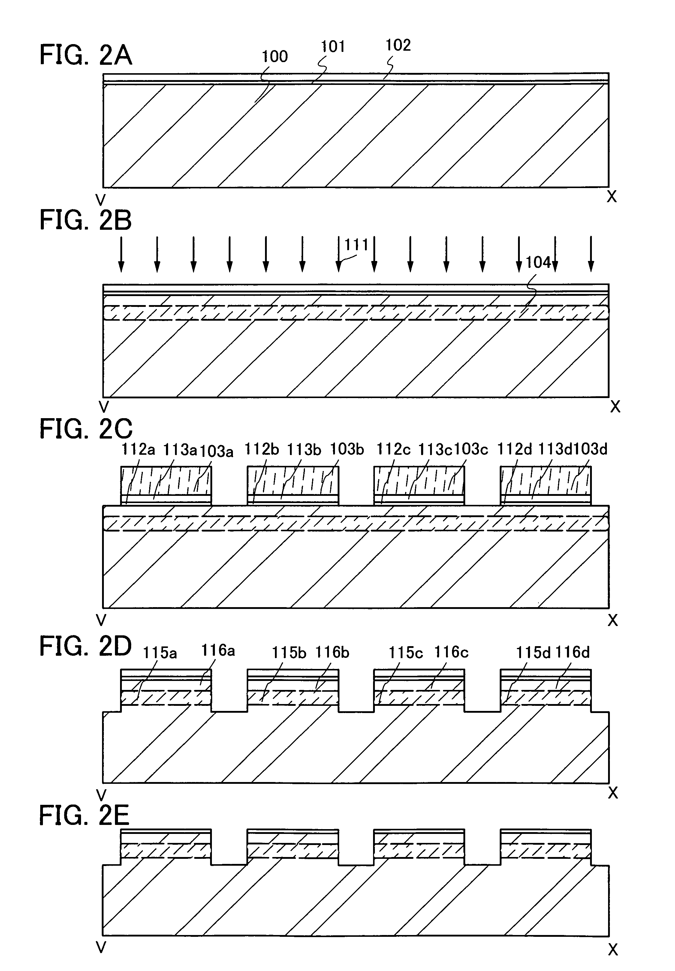
[0053]In this embodiment mode, a method for manufacturing a semiconductor device which aims to manufacture a semiconductor element (such as a metal insulator semiconductor (MIS) type electric field effect transistor (hereinafter also referred to as a “MISFET”)) and an integrated circuit that have high performance over a large-sized substrate with high throughput and high productivity will be described with reference to FIGS. 1A to 3D and FIGS. 5A to 5C. Specifically, a mode in which a semiconductor layer which forms a semiconductor element is transferred from a single crystal semiconductor substrate (hereinafter also referred to as a “bond wafer”) to a different substrate (hereinafter also referred to as a “base substrate”) will be described.
[0054]In this embodiment mode according to the present invention, when single crystal semiconductor layers are transferred from a single crystal semiconductor substrate (a bond wafer), the single crystal semiconductor substrate is etched selecti...
embodiment mode 2
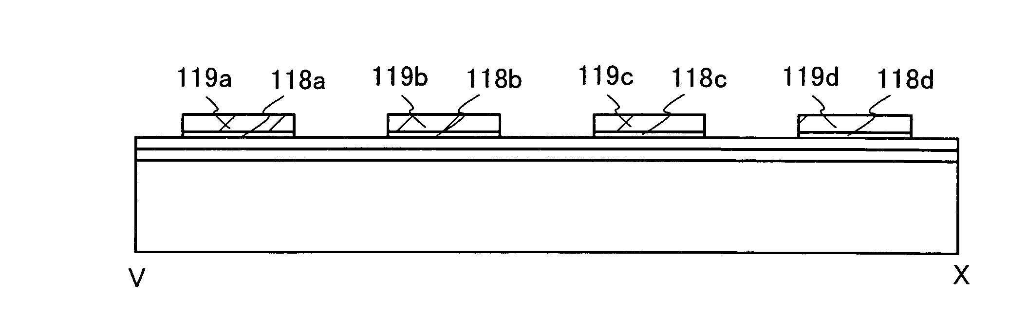
[0093]This embodiment mode will describe a manufacturing process of a bond wafer, which differs from that of FIGS. 2A to 2E, with reference to FIGS. 4A to 4D. In this embodiment mode, a bond wafer is irradiated with ions after groove processing.
[0094]In FIG. 4A, a silicon oxide film 101 and a silicon nitride film 102 are formed on a surface of a bond wafer 100. After that, the silicon oxide film 101 and the silicon nitride film 102 are etched using masks 103a, 103b, 103c, and 103d, and silicon oxide layers 112a, 112b, 112c, and 112d and silicon nitride layers 113a, 113b, 113c, and 113d are formed (see FIG. 4B).
[0095]Groove processing is performed on the bond wafer 100, using the silicon nitride layers 113a, 113b, 113c, and 113d as hard masks (see FIG. 4C). The groove processing is performed such that grooves correspond to the shapes of semiconductor layers of a semiconductor element formed over a base substrate. A depth to which the bond wafer 100 is etched is determined as appropri...
embodiment mode 3
[0100]This embodiment mode will describe an example in which a semiconductor integrated circuit is manufactured using the base substrate manufactured in any of Embodiment Modes 1 and 2. An inverter circuit will be described below as one structural example of a complementary metal oxide semiconductor (CMOS) circuit. Note that the present invention is not limited to such a simple circuit and can realize various integrated circuits such as a microprocessor.
[0101]FIGS. 6A to 12B each illustrate one mode of a semiconductor device using the present invention. FIGS. 6A, 7A, 8A, 9A, 10A, 11A, and 12A are plan views of an inverter circuit which is a semiconductor device of this embodiment mode, and FIGS. 6B, 7B, 8B, 9B, 10B, 11B, and 12B are cross-sectional views taken along line A-B of FIGS. 6A, 7A, 8A, 9A, 10A, 11A, and 12A. Note that several kinds of insulating layers are omitted in FIGS. 6A, 7A, 8A, 9A, 10A, 11A, and 12A. Note that repetitive description of the same portions or portions ...
PUM
 Abstract
Description
Claims
Application Information