Method for forming pattern, method for manufacturing semiconductor device and semiconductor device

a semiconductor device and pattern technology, applied in the direction of printing press parts, instruments, photomechanical equipment, etc., can solve the problems of difficult uniform application of resin over the entire surface of a first plate, increase in resin viscosity, and difficulty in forming electrically conductive thin films, etc., to achieve high accuracy, reduce viscosity of liquid composition, and high dispersibility

a semiconductor device and pattern technology, applied in the direction of printing press parts, instruments, photomechanical equipment, etc., can solve the problems of difficult uniform application of resin over the entire surface of a first plate, increase in resin viscosity, and difficulty in forming electrically conductive thin films, etc., to achieve high accuracy, reduce viscosity of liquid composition, and high dispersibility

US20080251844A1Inactive Publication Date: 2008-10-16SONY CORP

Image

  • Method for forming pattern, method for manufacturing semiconductor device and semiconductor device
  • Method for forming pattern, method for manufacturing semiconductor device and semiconductor device
  • Method for forming pattern, method for manufacturing semiconductor device and semiconductor device

Examples


example 1

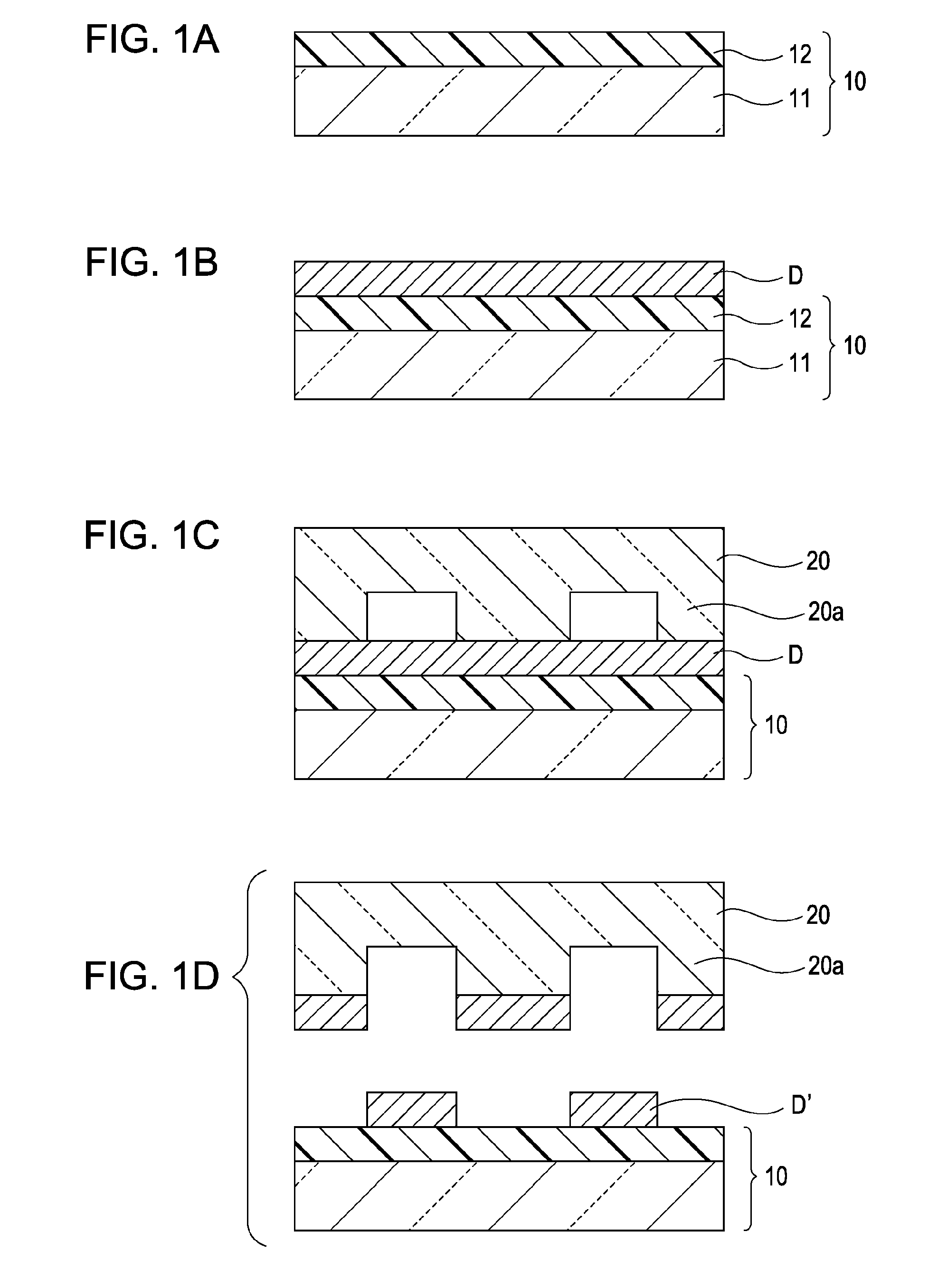
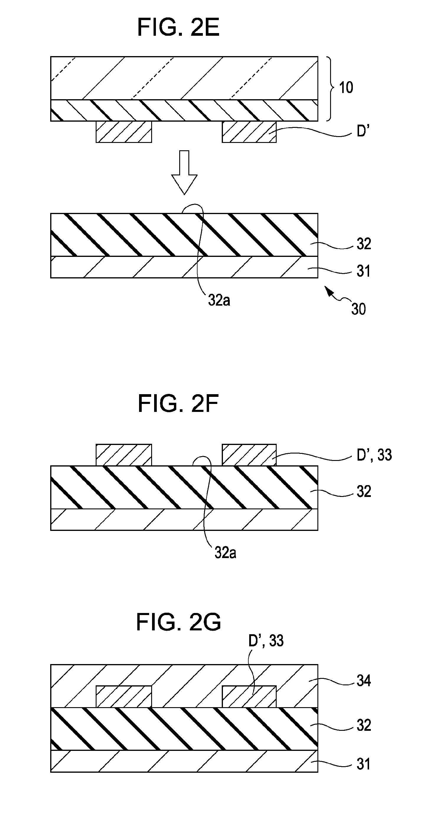
[0050]Similar to the above-mentioned embodiment, a first plate 10 (blanket) was formed on a glass substrate 11 by applying PDMS (Dow Corning Corporation, Silpot) using a spin coater and curing the PDMS by heating. Then, a liquid composition containing cyclohexane and silver nanoparticles dispersed in the cyclohexane to be 5 wt % was prepared, the surfaces of the silver nanoparticles (an average diameter of 10 nm) being treated with oleic acid. Next, an electrically conductive film D was formed on the first plate 10 by applying the liquid composition thereonto using a spin coater.

[0051]On the other hand, a second plate 20 composed of a glass plate was formed by applying a photoresist (KAYAKU MICROCHEM CO., LTD., SU-8) onto a glass substrate to form a photoresist film having a thickness of 5 μm using a spin-coater, and exposing and developing the photoresist film resulting in formation of a concave-convex pattern having a line-and-space (L / S) of 5 μm (aspect ratio 1:1) on a surface of...


PUM

PropertyMeasurementUnit
thicknessaaaaaaaaaa
thicknessaaaaaaaaaa
diameteraaaaaaaaaa

Abstract

A method for forming a pattern includes the step of forming an electrically conductive film by applying a liquid composition onto a first plate. The liquid composition includes an organic solvent and conductive particles surface-modified with a fatty acid or an aliphatic amine. Then, a second pattern, which is a reverse pattern of a first pattern, is formed on the first plate by pressing a second plate having a concave-convex pattern on a surface thereof on a surface of the first plate having the electrically conductive film on the surface thereof. Then, the first pattern of the electrically conductive film is transferred onto convex top faces of the second plate. Then, the second pattern is transferred onto a surface of a transfer substrate by pressing the surface of the first plate having the second pattern thereon on the surface of the transfer substrate.

Description

CROSS REFERENCES TO RELATED APPLICATIONS[0001]The present invention contains subject matter related to Japanese Patent Application JP 2007-106864 filed in the Japanese Patent Office on Apr. 16, 2007, the entire contents of which are incorporated herein by reference.BACKGROUND OF THE INVENTION[0002]1. Field of the Invention[0003]The present invention relates to a method for forming a pattern, a method for manufacturing a semiconductor device, and a semiconductor device, and, in particular, relates to a method for forming an electrically conductive pattern, a method for manufacturing a thin film transistor using the method for forming the electrically conductive pattern, and a thin film transistor.[0004]2. Description of the Related Art[0005]In the field of manufacturing semiconductor devices and image displays such as liquid crystal displays, many kinds of electrically conductive materials are used to form circuits. Since the density and definition have been further increased in rece...

Claims


Application Information

Patent Timeline
16 Oct 2008
Publication
US20080251844A1
IPC
H01L29/786; H01L21/336
CPC
B82Y10/00; B82Y40/00; G03F7/0002; H01L51/0022; H01L51/0545; H05K2203/122; H05K3/046; H05K3/207
Inventors
NOMOTO, AKIHIRO; NOMOTO, KAZUMASA