Hydrogen ashing enhanced with water vapor and diluent gas

a technology of hydrogen ashing and water vapor, which is applied in the direction of photomechanical equipment, instruments, and semiconductor/solid-state device details, etc., can solve the problems of difficult etching, difficult hydrogen ashing, and relatively fragile porous dielectric materials

Active Publication Date: 2008-10-23
APPLIED MATERIALS INC
View PDF15 Cites 255 Cited by
  • Summary
  • Abstract
  • Description
  • Claims
  • Application Information

AI Technical Summary

Problems solved by technology

Ashing has however presented difficulties when applied to more advanced low-k dielectrics needed for advanced integrated circuits.
Oxygen ashing of these materials causes many problems.
Porous dielectric materials are relatively fragile and even more prone to damage from the oxygen plasma due to partial penetration of oxygen into the pores and the collapse of the pores.
However, hydrogen ashing is a very slow process due to a low reducing reaction rate and the low hydrogen radical density generated in an environment of only reducing gases.
While oxygen ashing may require 20 seconds of processing, hydrogen ashing may require ten times as long, clearly an economic disadvantage.
However, porous low-k materials are sensitive even to small amounts of oxygen, which can remove significant carbon from the silicon oxycarbide material and collapse the pore structure and increase the dielectric constant.

Method used


Image

  • Hydrogen ashing enhanced with water vapor and diluent gas
  • Hydrogen ashing enhanced with water vapor and diluent gas
  • Hydrogen ashing enhanced with water vapor and diluent gas

Examples


Embodiment Construction

[0014]The addition of water vapor and a large amount of argon or helium to the hydrogen-based ashing plasma greatly increases the concentration of hydrogen radicals and increases the ashing rate with reduced damage to low-k dielectrics.

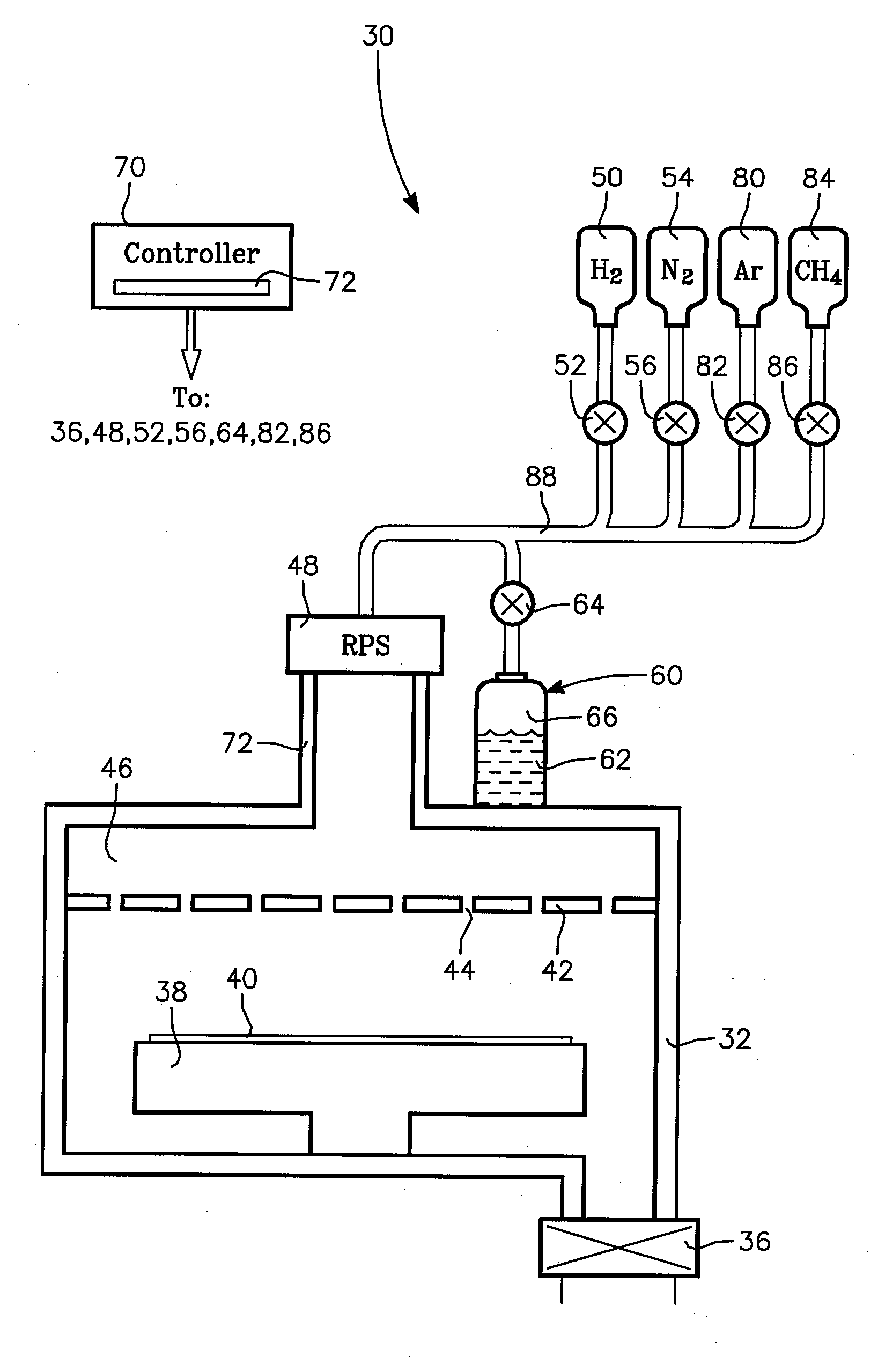
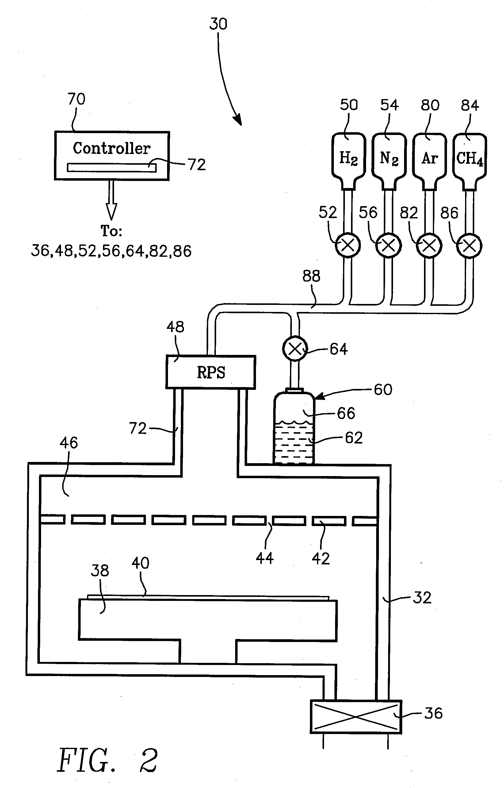
[0015]The invention may be practiced in a plasma ashing reactor 30, schematically illustrated in the cross-sectional view of FIG. 2. A vacuum processing chamber 32 is pumped by a vacuum pumping system 36 to the low Torr range. A pedestal 38 within the chamber 32 supports a wafer 40 to be ashed in opposition to a gas showerhead 42 supplying a process gas through a large number of apertures 44.

[0016]The process gas is supplied to a manifold 46 in back of the showerhead 42 through a remote plasma source 48 which excites the process gas into a plasma. The remote plasma source 48 may be located a distance away from the vacuum chamber 48 but is still considered ancillary to it since the gas containing the plasma generated in the remote plasma source 48 flow...


PUM

PropertyMeasurementUnit
dielectric constantaaaaaaaaaa
dielectric constantsaaaaaaaaaa

Abstract

An oxygen-free hydrogen plasma ashing process particularly useful for low-k dielectric materials based on hydrogenated silicon oxycarbide materials. The main ashing step includes exposing a previously etched dielectric layer to a plasma of hydrogen and optional nitrogen, a larger amount of water vapor, and a yet larger amount of argon or helium. Especially for porous low-k dielectrics, the main ashing plasma additionally contains a hydrocarbon gas such as methane. The main ashing may be preceded by a short surface treatment by a plasma of a hydrogen-containing reducing gas such as hydrogen and optional nitrogen.

Description

FIELD OF THE INVENTION[0001]The invention relates generally to plasma etching of materials in the fabrication of integrated circuits. In particular, the invention relates to ashing of photoresist.BACKGROUND ART[0002]Plasma etching is widely used in the fabrication of silicon integrated circuits. One of its uses, often called dielectric etching, is used to form holes through dielectric layers to provide vertical electrical connections between different levels of the integrated circuit. A prototypical via structure is schematically illustrated in the cross-sectional view of FIG. 1. A lower dielectric layer 10 formed on the surface of a wafer has a conductive feature 12 formed in its surface. An upper dielectric layer 14 is deposited over the lower dielectric layer 10 and its conductive feature 12. A planar photoresist layer 16 is spun onto the so far unpatterned upper dielectric layer 14 and a stepper photographically exposes it according to a pattern of radiation to form a mask apert...

Claims


Application Information

Patent Timeline
Patent Type & Authority Applications(United States)
IPC IPC(8): H01L21/302
CPCH01L21/02063H01L21/76814H01L21/31138H01L21/306H01L21/3065
Inventor YANG, CHAN-SYUNLEE, CHANGHUN
Owner APPLIED MATERIALS INC
Why Eureka
Try Eureka