Pattern forming method performing multiple exposure so that total amount of exposure exceeds threshold

a pattern and forming technology, applied in the field of pattern forming methods, can solve the problems of wiring degradation, limited range of exposure conditions, small margin, etc., and achieve the effect of low cost and easy forming

Inactive Publication Date: 2008-10-30
ELPIDA MEMORY INC
View PDF8 Cites 18 Cited by
  • Summary
  • Abstract
  • Description
  • Claims
  • Application Information

AI Technical Summary

Benefits of technology

[0018]In light of the above circumstances, an object of the present invention is to provide a pattern forming technique employing an easy manufacturing method including a very small number of processes, in which even when a fine four-corner pattern having a width close to a limit resolution is formed by utilizing the advantage of double exposure, a circular patter is hardly produced, and a pattern closer to a four-corner shape can be formed in comparison with the conventional techniques, that is, a fine pattern inconformity with a desired shape can be formed very easily at low cost, without providing an irregular shape.
[0019]Another object of the present invention is to provide a pattern forming technique by which even when forming fine patterns, the interval between the patterns can be reduced so as to provide a high density arrangement, and to form the patterns with a narrower pitch in comparison with the possible interval in the conventional techniques.
[0020]Another object of the present invention is to provide a pattern forming technique by which even when forming fine patterns, the dimensional accuracy with respect to pattern formation is high, so that electric resistance at each formed part to be connected to wiring can be low, thereby preventing the wiring from being degraded due to electric current concentration.

Problems solved by technology

That is, when forming a fine contact hole corresponding to almost limit resolution, the presently-known photoresist technique employing reduced-projection exposure causes (i) a first problem in which the diameter of the formed contact-hole pattern varies from a desired value, and (ii) a second problem in which the focus margin is small, that is, the range having an appropriate exposure condition is limited.
This circumstance further causes (iii) a third problem in which the part which contacts the wiring has a high electric resistance, and (iv) a fourth problem in which electric current tends to concentrate at the part (having a circular pattern shape) which contacts the wiring, which tends to cause a degradation of the wiring.
However, when the hole pattern is formed by using the above-described method, another problem occurs as explained below.
Therefore, the method explained with reference to FIGS. 31 to 35 has lots of processes required for processing, and is thus complex.

Method used


Image

  • Pattern forming method performing multiple exposure so that total amount of exposure exceeds threshold
  • Pattern forming method performing multiple exposure so that total amount of exposure exceeds threshold
  • Pattern forming method performing multiple exposure so that total amount of exposure exceeds threshold

Examples


concrete examples

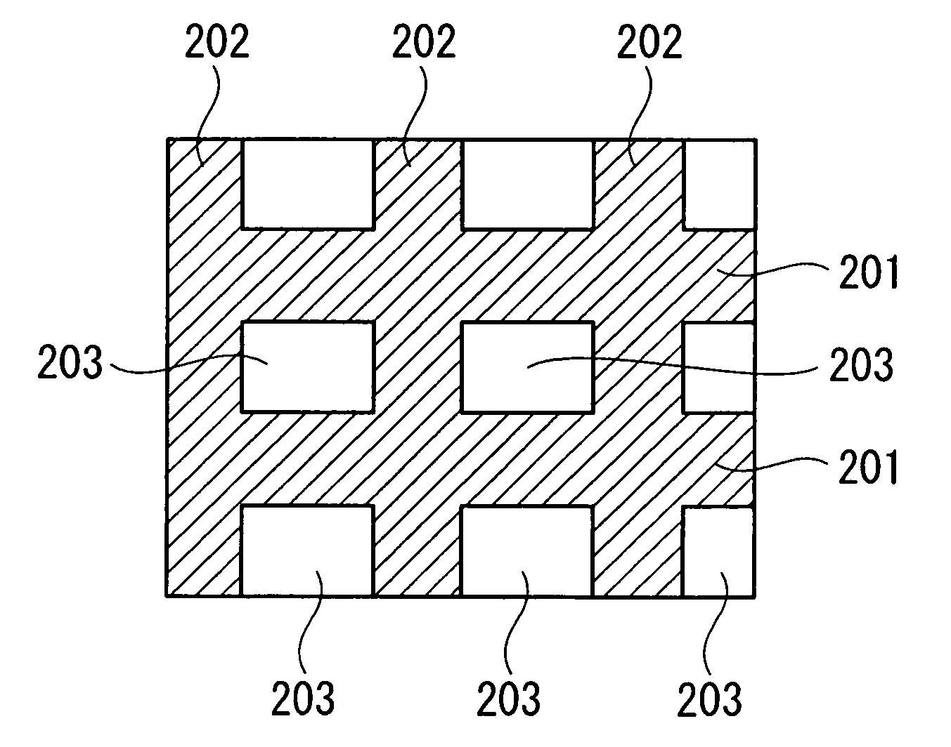
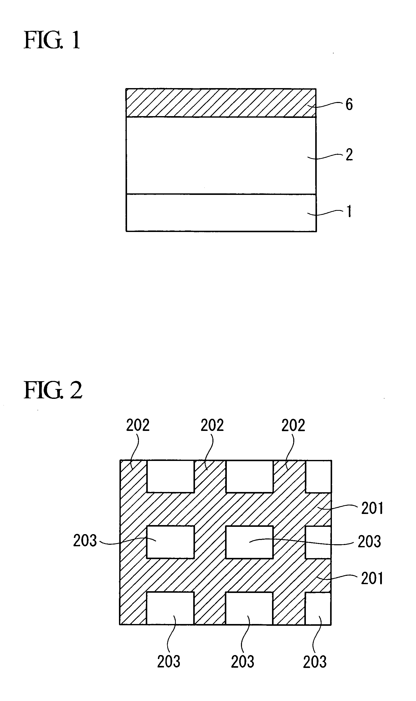
[0176]A concrete example which was actually performed will be described below. In a preparatory process, a transistor structure as shown in FIG. 29 is formed on a semiconductor substrate, and capacitance contact plugs 90 are formed through the second inter-layer insulating film.

[0177]In the next step, a silicon nitride film is formed on the second inter-layer insulating film, and a cylinder inter-layer insulating film, which has a thickness of 2500 nm and is made of a silicon oxide film, is further formed thereon.

[0178]The cylinder inter-layer insulating film is formed by means of a PECVD (plasma-enhanced CVD) method using monosilane (SiH4) and nitrogen monoxide (N2O), or may be formed by a PECVD method using TEOS (Si(OC2H5)4) and oxygen (O2).

[0179]Next, deep-hole cylinders, each passing through the cylinder inter-layer insulating film and the silicon nitride film, are provided by means of photolithography and dry etching, so that the surface of each capacitance contact plug is expo...


PUM

PropertyMeasurementUnit
thresholdaaaaaaaaaa
thresholdaaaaaaaaaa
wavelengthaaaaaaaaaa

Abstract

A pattern forming method includes forming a resist film on a target film to be processed, which is formed on a substrate; and forming a basic pattern part in the resist film by multiple exposure using photomasks, wherein each exposure process is performed at an amount of exposure smaller than a threshold assigned to the resist film; and the resist film is developed after the total sum of the amounts of exposure through a plurality of exposure processes exceeds the threshold, so that the basic pattern part including a hole shape, which corresponds to each area where the total amount of exposure through the exposure processes via the photomasks exceeds the threshold, is formed in the resist film. The method also includes performing etching via the basic pattern part so as to form a desired pattern in the target film.

Description

BACKGROUND OF THE INVENTION[0001]1. Field of the Invention[0002]The present invention relates to a pattern forming method for forming a fine hole or line pattern on a film to be processed with a high resolution.[0003]Priority is claimed on Japanese Patent Application No. 2007-115410, filed Apr. 25, 2007, the contents of which are incorporated herein by reference.[0004]2. Description of the Related Art[0005]In recent years, a large-scale integrated circuit (LSI) in which a large number of MOS transistors, resistors, capacitors, and the like are integrated on a single chip is employed in a main part of a computer or an electric device. In a device such as DRAM (dynamic random access memory) among LSIs, fine patterning has been rapidly developed, and accordingly, wiring lines or contact holes with respect to MOS transistors or registers have been reduced in size almost to the limit of the exposure techniques used.[0006]As a technique for forming such a fine wiring pattern, Japanese Une...

Claims


Application Information

Patent Timeline
Patent Type & Authority Applications(United States)
IPC IPC(8): G03F7/20
CPCG03F7/2022H01L21/0274
Inventor SAITO, MASAYOSHIOHARA, SHINJI
Owner ELPIDA MEMORY INC
Why Eureka
Try Eureka