

RECESSED GATE CHANNEL WITH LOW Vt CORNER
a gate channel and low vt technology, applied in the field of semiconductor cmos devices, can solve the problems of introducing history, degrading the short channel effect of fet devices, and convex channel corners with poor transport properties, and achieve the effect of low v
- Summary
- Abstract
- Description
- Claims
- Application Information
AI Technical Summary
Benefits of technology
Problems solved by technology
Method used
Image

Examples
first embodiment
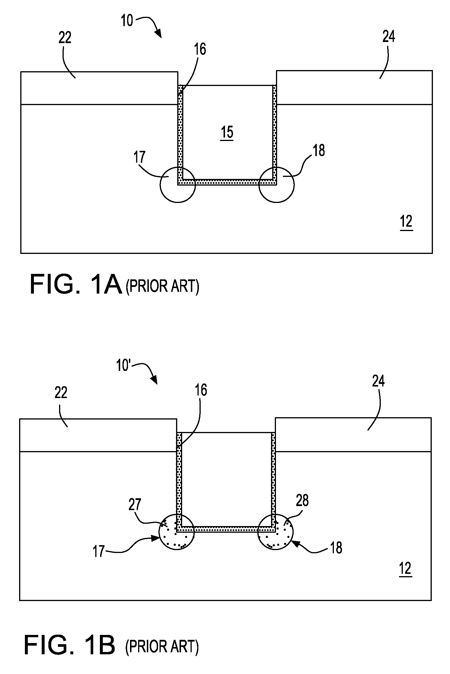
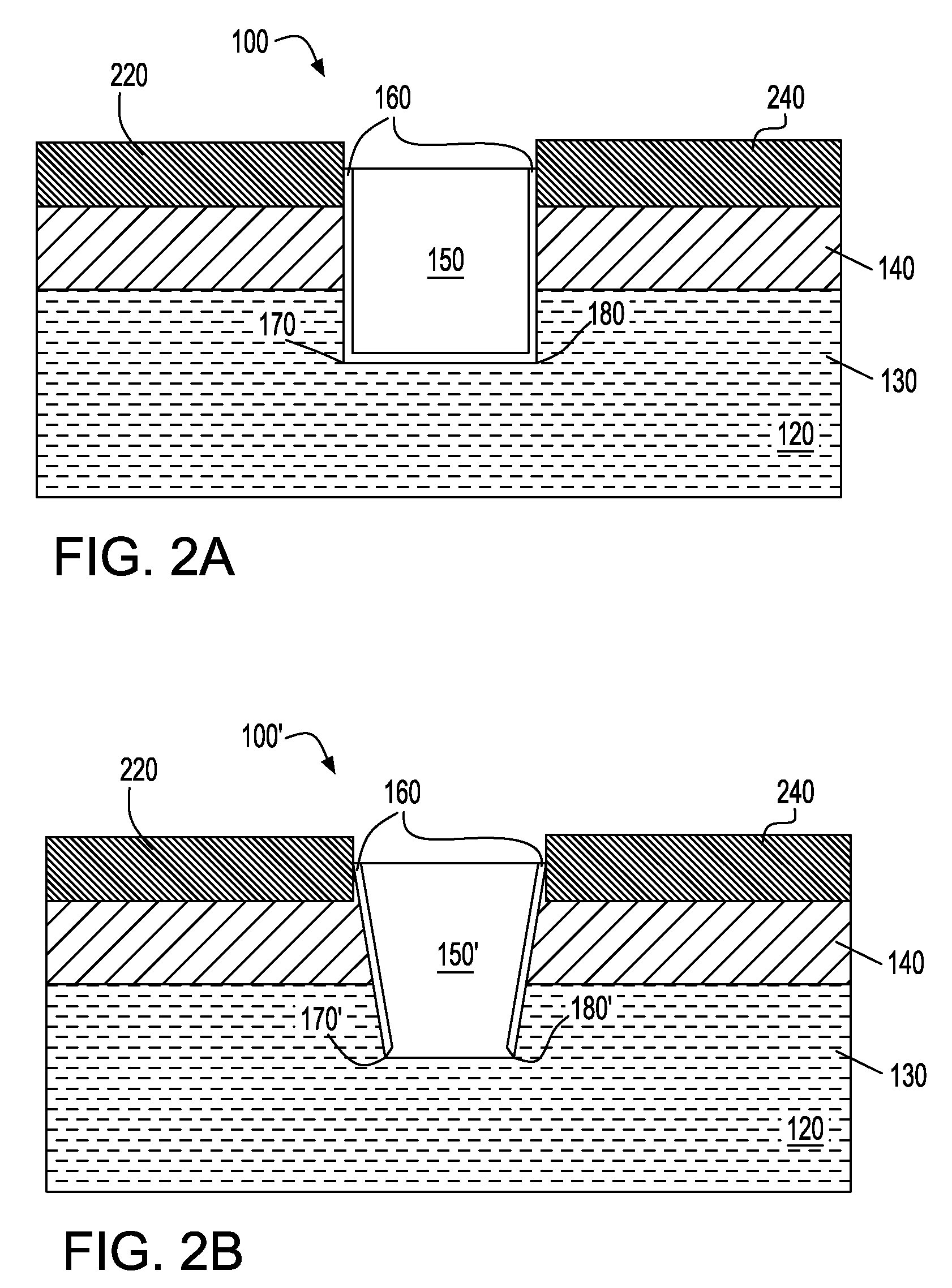
[0065]FIG. 2A illustrates the FET device structure 100 having a recessed gate 150 according to the present invention. As shown in FIG. 2A, the FET device structure 100 is formed on a substrate 120 having a lower low doped substrate layer 130 of a first thickness and a very high doped body layer 140 of a second thickness formed on top such that the recessed gate 150 includes sidewalls extending through the high-doped body layer 140 with the corner regions 170, 180 of the device formed in the lower low doped substrate layer 130. The substrate 120 may comprise a bulk semiconductor substrate including, for example, Si, SiGe, SiC, SiGeC, GaAs, InP, InAs and other semiconductors, or layered semiconductors such as silicon-on-insulators (SOI), SiC-on-insulator (SiCOI) or silicon germanium-on-insulators (SGOI). For purposes of description, substrate 120 is a Si-containing semiconductor substrate including a first layer 130 lightly doped with material of a first conductivity type, e.g., light...
second embodiment
[0074]FIG. 3A illustrates the FET device structure 200 having a recessed gate 250 according to the present invention. As shown in FIG. 3A, the FET device structure 100 is formed on a Silicon-On-Insulator (SOI) structure that includes an insulating layer 125, i.e., buried oxide region (BOX), that electrically isolates a top Si-containing layer 145 from a bottom Si-containing layer 135. The top Si-containing, i.e., the SOI layer, serves as the area in which electronic devices such as the MOSFETs of the invention can be fabricated.
[0075]The SOI structure shown in FIG. 3A is fabricated using techniques well known to those skilled in the art. For example, the SOI structure illustrated in FIG. 4 may be formed by a thermal bonding process, or alternatively, the SOI structure may be formed by an oxygen implantation process which is referred to in the art as a separation by implantation of oxygen (SIMOX) process. In some embodiments, the SOI structure is formed by depositing or thermally gro...
third embodiment
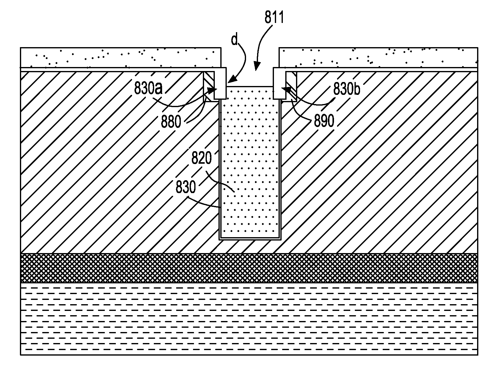
[0081]FIG. 4A illustrates a FET device structure 300 according to the invention which includes the FET device structure 250′ having “backgated” corners. That is, the device structure shown in FIG. 4A includes a recessed gate such as the recessed tapered trench gate 250′, and is formed on a Silicon-On-Insulator (SOI) structure that includes an insulating layer 125, i.e., buried oxide region (BOX), and, a backgate isolation layer 310 formed on top of the insulating layer 125 and having a back gate portion 350 including a thin backgate dielectric, e.g., oxide layer, 320. The back gate isolation layer 310 is any suitable dielectric, typically silicon dioxide or silicon nitride. In this embodiment, the back-gate 350 is used to maximize back gate control in the ultra-thin undoped or lightly doped channel region 136, and may comprise a doped-polysilcon back gate electrode with p+doping and n+doping, or may comprise a refractory metal such a tungsten. Particularly, the back-gate 350 is used...
PUM
 Abstract
Description
Claims
Application Information