Controller for Non-Volatile Memories and Methods of Operating the Memory Controller

US20080270680A1Active Publication Date: 2008-10-30CHANG CHEE KENG

Image

  • Controller for Non-Volatile Memories and Methods of Operating the Memory Controller
  • Controller for Non-Volatile Memories and Methods of Operating the Memory Controller
  • Controller for Non-Volatile Memories and Methods of Operating the Memory Controller

Examples


Embodiment Construction

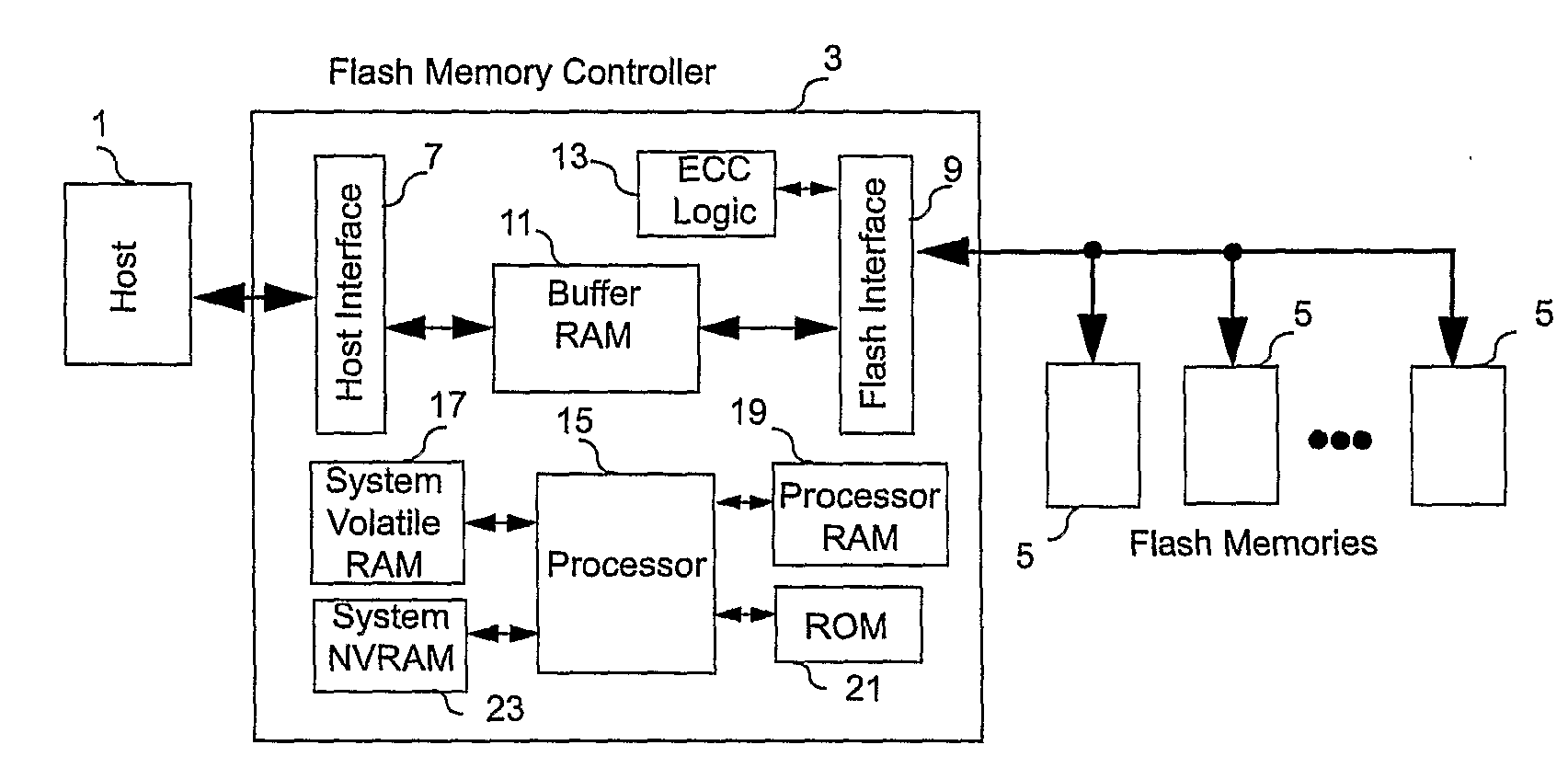
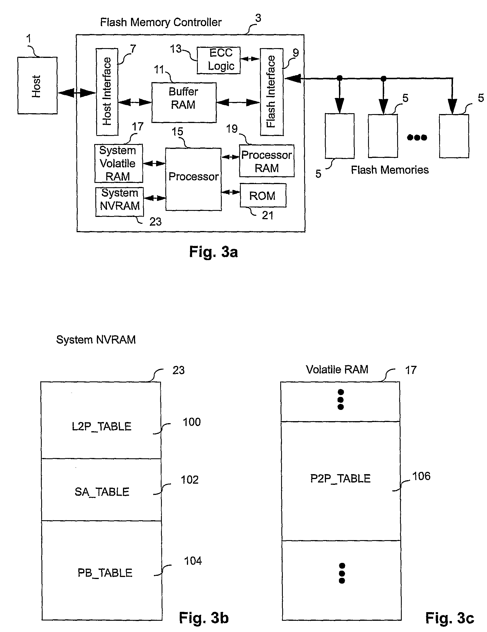
[0096]An embodiment of the present invention will now be described. The flash memory system typically has blocks shown in FIG. 3a, and the corresponding elements of the embodiment are given the same reference numbers as in FIG. 2. All elements shown in FIG. 3a are the same as FIG. 2, except that there is an additional system NVRAM memory device 23 incorporated into the flash controller. In FIG. 3a, the system NVRAM 23 is illustrated as a component within the flash controller 3, e.g. provided as part of a single integrated circuit which also integrates the other components of the flash controller 3. However, optionally, the NVRAM memory device 23 may be an external component connected to the flash controller 3 via a dedicated interface port.

[0097]One possible form of the embodiment is to assemble the flash controller 3 and the flash memories 5 into a single physical unit such as a memory card or a flash drive, and the interface to the host 1 (e.g. a personal computer) comprises a mat...


PUM


Abstract

A non-volatile memory system (3) is proposed consisting of a first non-volatile flash memory (5) having a plurality of blocks, each block having a plurality of pages, each block being erasable and each page being programmable, and a second non-volatile random access memory (23) having a plurality of randomly accessible bytes. The second non-volatile memory (23) stores data for mapping logical blocks to physical blocks and status information of logical blocks. Each logical block has an associated physical page pointer stored in the second non-volatile memory (23) that identifies the next free physical page of the mapped physical block to be written. The page pointer is incremented after every page write to the physical block, allowing all physical pages to be fully utilized for page writes. Furthermore, a method of writing and reading data is disclosed whereby the most recently written physical page associated with a logical address is identifiable by the memory system without programming flags into superseded pages, or recording time stamp values in any physical page or block of the first non-volatile memory (5). Furthermore, a method is provided for a logical block to be mapped to two physical blocks instead of one to provide additional space for page writes, resulting in reduction in page copy operations, thereby increasing the performance of the system.

Description

FIELD OF THE INVENTION[0001]This invention relates to a data storage system employing a solid state (i.e. semiconductor-type) non-volatile memory, such as a flash memory, and methods of operating such a memory. In particular, it relates to the construction, architecture and techniques of a flash memory controller for accessing such a non-volatile flash memory.BACKGROUND OF THE INVENTION[0002]Flash memory is a form of EEPROM (Electrically Erasable and Programmable Read Only Memory) that allows multiple memory locations to be erased or written in one programming operation. The memory is commonly used as a mass data storage subsystem for electronic devices, such as memory cards, USB (Universal Serial Bus) flash drives and solid-state drives as replacements of hard disk drives.[0003]A flash memory device consists of one or more arrays of transistor cells as its data storage units. Each of those cells is capable of keeping one or more bits of data even if the electric power supply is cut...

Claims


Application Information

Patent Timeline
30 Oct 2008
Publication
US20080270680A1
IPC
G06F12/02
CPC
G11C16/10; G11C2029/1806
Inventors
CHANG, CHEE KENG