Organic Light Emitting Device

Active Publication Date: 2008-11-06
ROHM CO LTD +1
View PDF29 Cites 50 Cited by
  • Summary
  • Abstract
  • Description
  • Claims
  • Application Information

AI Technical Summary

Benefits of technology

[0010]In view of the above problem, the object of the present invention is to provide an organic light emitting device which can reduce the angle dependency of the emission brightness a

Problems solved by technology

In this structure, a phenomenon of an optical interference effect or light confinement in a high refractive index medium, such as the emission layer of an organic film, the substrate, and the electrode, by a total reflection may be occurred, and as a result, angle dependency of emission brightness and emission spectrum, film thickness dependency, and deterioration of light use efficiency are observed.
This problem is occurred in the above organic light emitting device which is the multiphoton device having a plurality of emission layers.
This means that an allowable fluctuation of the film thickness in a manufacturing process of the organic light emitting device becomes smaller, and it is directly linked to a productivity problem.
Particularly, in the above organic light emitting device having a structure in which the emission layers and the equipotential surface forming layers or the charge generating layers are stacked, accuracy and inevitability of the film thickness control further increase because film thickness abnormality of any layer may affect on even the optical position of other layers.
That is, in a organic light emitting device having only one emission layer, the fluctuation of the emission brightness and the emission color with r

Method used


Image

  • Organic Light Emitting Device
  • Organic Light Emitting Device
  • Organic Light Emitting Device

Examples


example 1

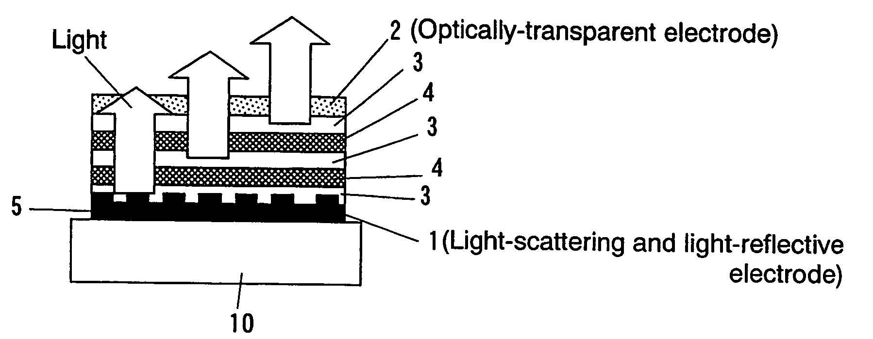
[0083]Silica particle slurry which was 500 nm in average grain diameter was applied on a substrate 10 of alkali-free glass and was dried, and then it was baked at 600 degrees for 50 minutes. Average plane roughness of the surface of the substrate 10 was 130 nm, and maximum vertical interval thereof was about 2 μm. Then, the surface of the substrate 10 was cleaned by ultrasonic cleaning using acetone and isopropyl alcohol, and UV / O3 cleaning, and then a film of Cr was formed on the surface of the substrate 10 to a thickness of 2200 Å by sputtering, and a Al film which was 800 Å in thickness was formed thereon by vacuum deposition, whereby an light-scattering and light-reflective electrode (cathode 2) was formed.

[0084]Next, the substrate 10 was set to a vacuum evaporation system, and an electron injection layer was formed on the cathode 2 by co-depositing bathocuproine (manufactured by DOJINDO LABORATORIES Corporation) and Cs at molar ratio of 1 to 1, to a thickness of 200 Å, under a ...

example 2

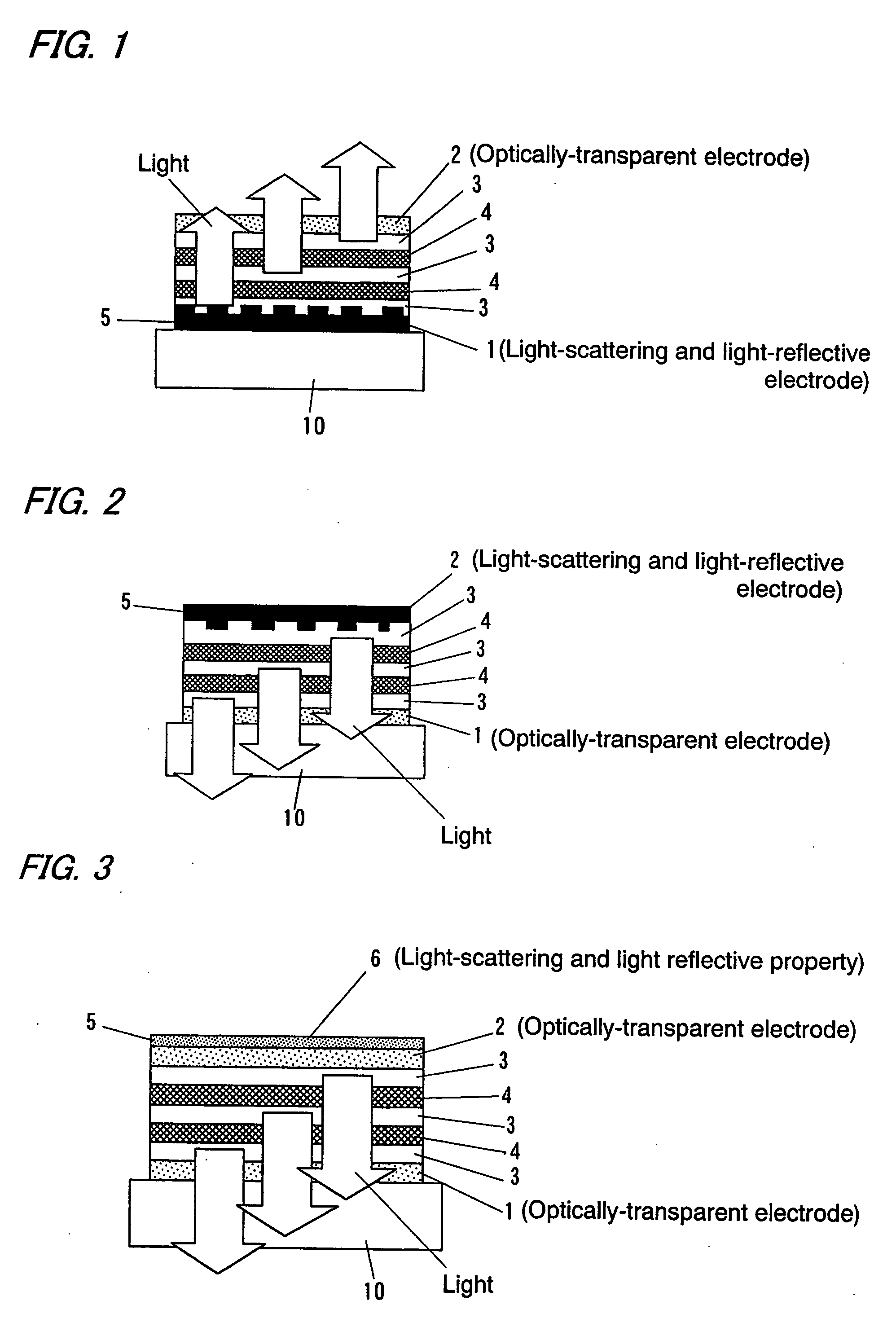
[0087]An ITO thin film was formed by sputtering on a surface of a substrate 10 formed by an alkali-free substrate glass plate having a thickness of 0.7 mm, whereby an optically-transparent electrode (cathode 2) having a thickness of 1100 Å and sheet resistance of 12Ω / □ was formed. The glass substrate 10 and the ITO cathode 2 was etched and cut into a shape shown in FIG. 11A, and then it was cleaned by ultrasonic cleaning using pure water, acetone, and isopropyl alcohol, for ten minutes, respectively, and then it was cleaned by steam cleaning using isopropyl alcohol steam for two minutes and it was dried, and then it was cleaned by UV ozone wash for 30 minutes.

[0088]Then, the surface of the substrate 10 opposite to the surface where the cathode 2 was formed was roughened by sandblast with roughness of #220, and then an Al film having a thickness of 1000 Å was formed on the roughened surface, whereby a light-scattering and light-reflective element 6 was formed.

[0089]After that, as is ...

example 3

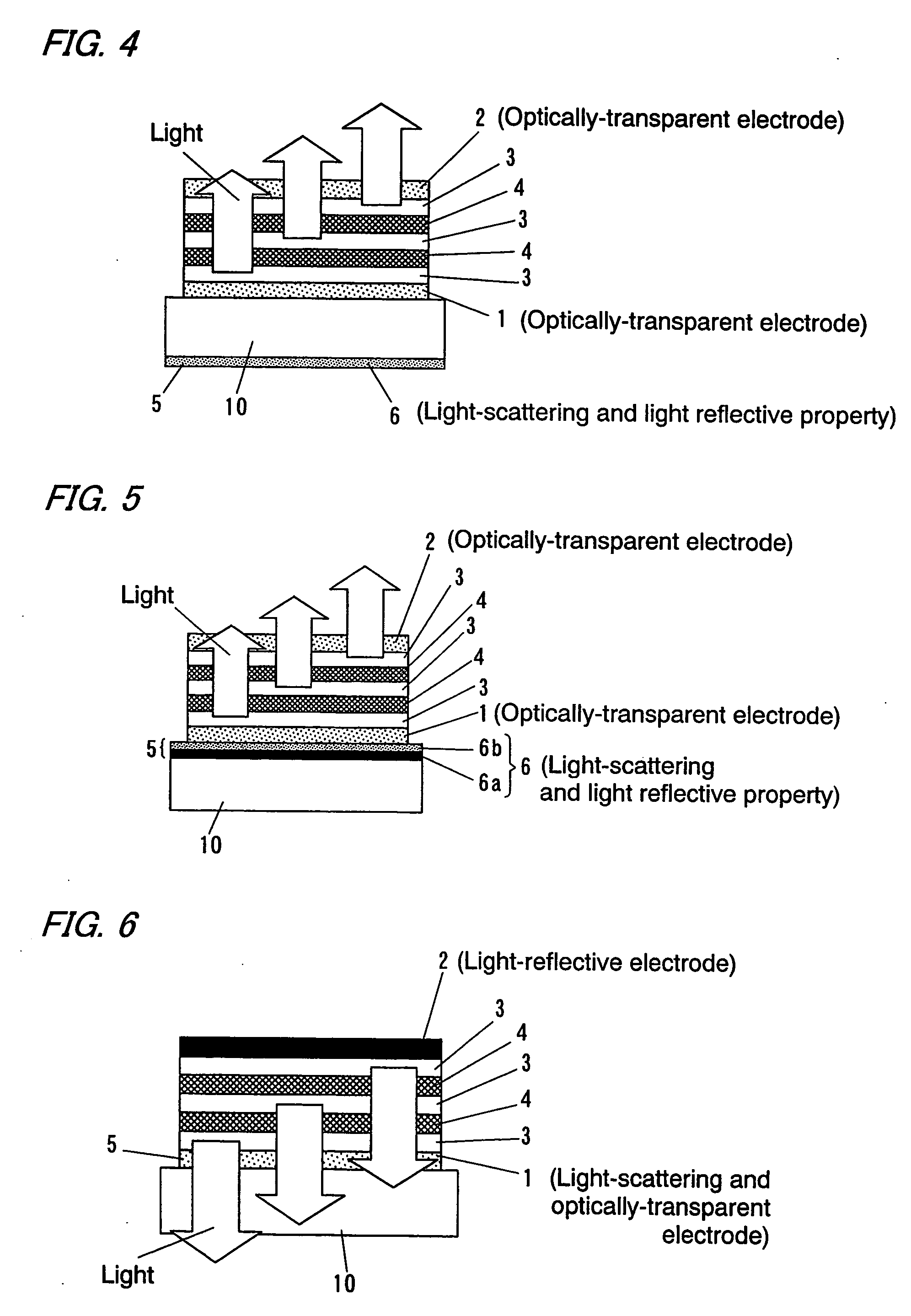
[0090]As is the case with the second example, an organic light emitting device was manufactured according to the example 1, using the substrate 10 on which the light-scattering and light-reflective element 6 was formed on the opposite surface of the cathode 2. However, a film thickness and a layer construction were as follows. An electron injection layer having a thickness of 200 Å and comprising a co-deposition layer of bathocuproine and Cs of molar ratio of 1 to 1, an electron transport layer having a thickness of 500 Å and comprising only bathocuproine, an emission layer having a thickness of 300 Å and formed by co-deposition of Alq and rubrene with 7% weight fraction of rubrene, a hole transport layer having a thickness of 400 Å, a charge generating layer 4 having a thickness of 100 Å and comprising vanadium oxide, an electron injection layer having a thickness of 200 Å and comprising a co-vapor deposition layer of bathocuproine and Cs of molar ratio of 1 to 1, an emission layer...


PUM


Abstract

The present invention provides an organic light emitting device which can reduce the angle dependency of the emission brightness and the emission color, and has a small change in the emission brightness and the emission color with respect to film thickness fluctuations, and can increase use efficiency of the light. The organic light emitting device of the present invention has a plurality of emission layers 3 between an anode 1 and a cathode 2, and the emission layers 3 are separated from each other by an equipotential surface forming layer 4 or a charge generating layer 4. The feature of the present invention resides in that the organic light emitting device has, at least either inside or outside the device, a light scattering means 5 for scattering light emitted from the emission layers 3. The organic light emitting device can reduce the angle dependency of the emission brightness and the emission color by outputting the light emitted from the emission layers in a condition where the light is scattered by the light scattering means.

Description

TECHNICAL FIELD[0001]The present invention relates to a light emitting device which is used for a flat panel display, a back light of a liquid crystal display (LCD), a light source of lighting, illuminations, and a light source for a sign.BACKGROUND ART[0002]Generally, in an organic light emitting device known and described as an organic electroluminescence device (an organic EL device), an anode which is a transparent electrode, a hole transport layer, an organic emission layer, an electron injection layer, and a cathode are stacked on one side of a transparent substrate in this order. When a voltage is applied between the anode and the cathode, an electron injected into the emission layer through the electron injection layer and a hole injected into the emission layer through the hole transport layer recombine in the emission layer, and an excited state occurs and light is emitted. The light emitted from the emission layer is taken out through the transparent electrode and the tra...

Claims


Application Information

Patent Timeline
IPC IPC(8): H01J1/63H01L27/32H01L51/52H05B33/02H05B33/12H05B33/14H05B33/26
CPCH01L27/3209H01L51/5206H01L51/5203H01L51/5268H01L51/5278H01L51/5221H10K59/32H10K50/81H10K50/818H10K50/828H10K50/854H10K50/19H05B33/26H05B33/02H05B33/14H10K50/805H10K50/82
Inventor IDE, NOBUHIROENDO, JUNKIDO, JUNJI
Owner ROHM CO LTD
Why Eureka
Try Eureka