
Organic electroluminescent device and method for preparing the same

a technology of electroluminescent devices and organic materials, which is applied in the manufacture of electrode systems, electric discharge tubes/lamps, and discharge tubes luminescent screens, etc., can solve the problems of reducing the effective display aperture ratio, affecting the electric power consumed for driving and life time, and the reduction of the display aperture ratio. , to achieve the effect of improving the electron injection characteristic and preventing damage to the organic material layer

Inactive Publication Date: 2008-11-20
LG CHEM LTD
View PDF38 Cites 56 Cited by
  • Summary
  • Abstract
  • Description
  • Claims
  • Application Information

AI Technical Summary

Benefits of technology

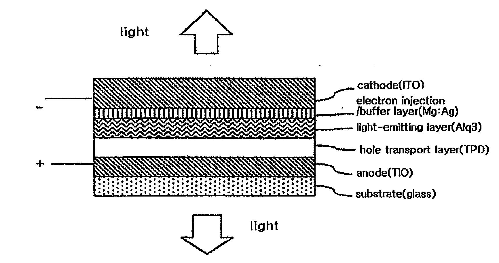
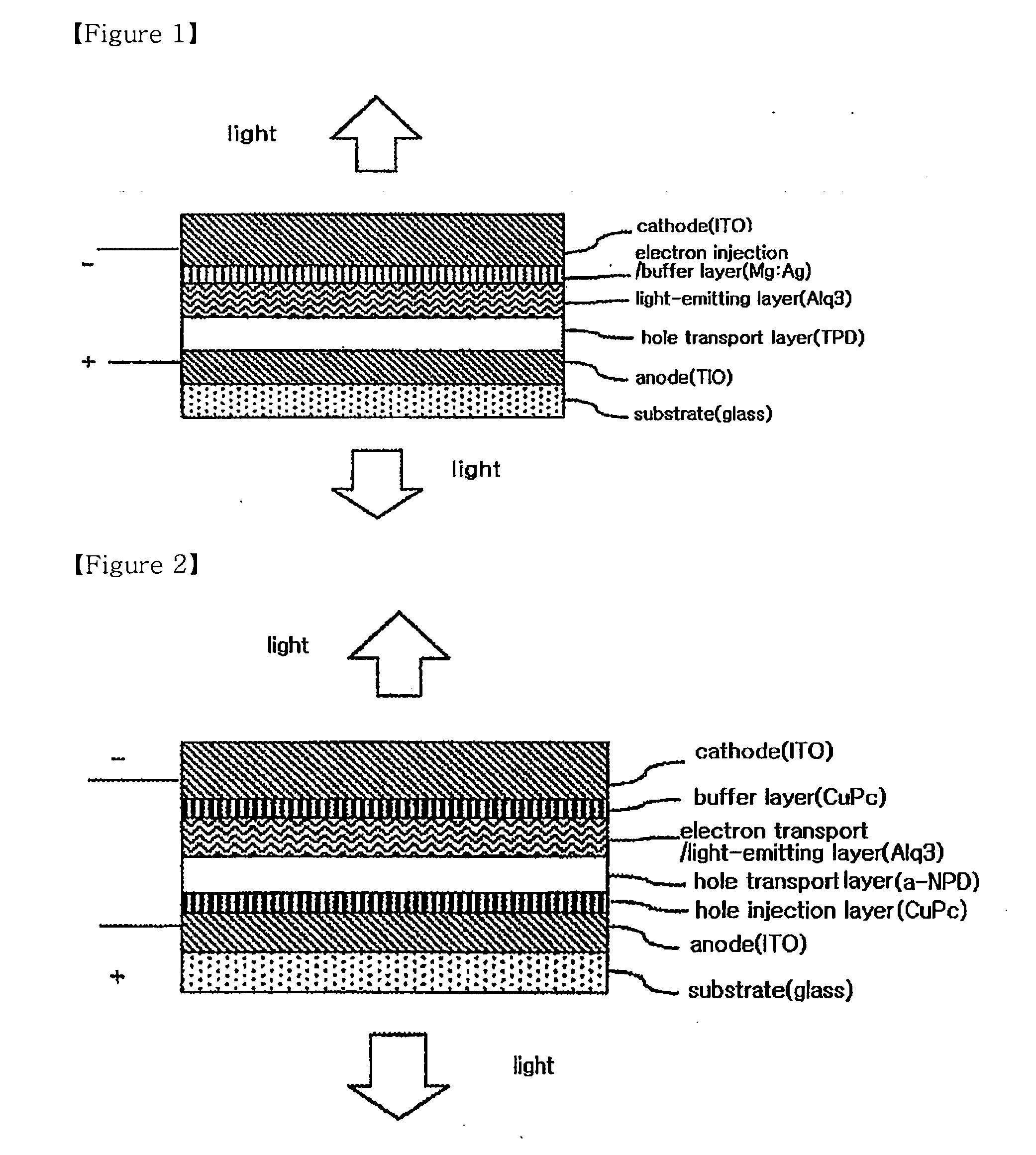
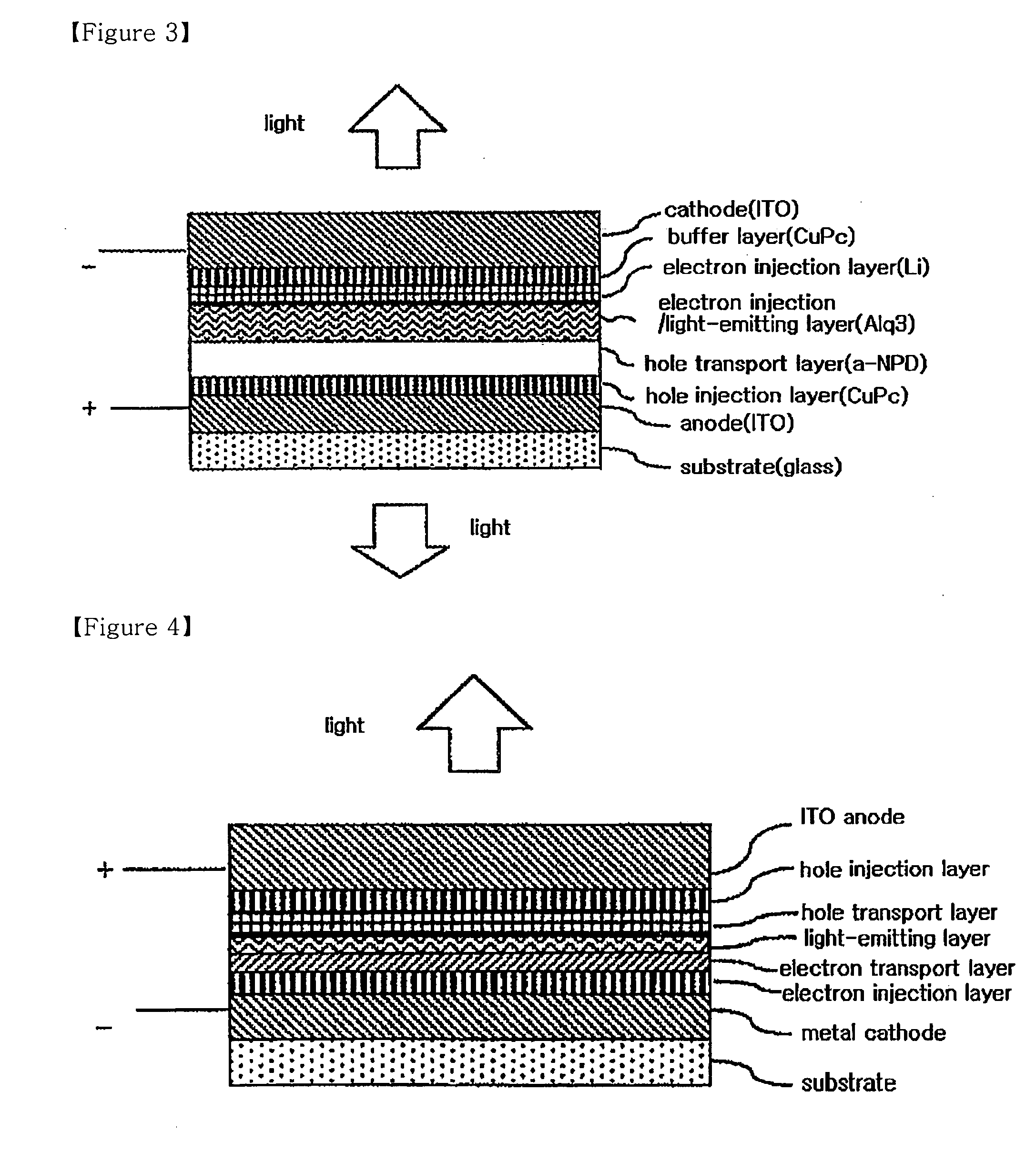
[0024]The organic electroluminescent device according to the present invention comprises an organic material layer comprising a compound having a functional group selected from the group consisting of an imidazole group, an oxazole group and thiazole group between the cathode and the light-emitting layer, thus having an improved electron injection characteristic to provide an organic electroluminescent device of an inverted structure operating at a low voltage. In addition, the organic electroluminescent device according to the present invention comprises a buffer layer between the light-emitting layer and the anode, thus preventing damage to the organic material layer, which can occur when forming the anode on the organic material layer in a process of fabricating the organic electroluminescent device of the inverted structure.

Problems solved by technology

When the active matrix organic electroluminescent device displays having this backplane are fabricated to have the bottom emission structure, a portion of light emitted toward the substrate is blocked by the TFT array, resulting in a reduction in the effective display aperture ratio.
This problem becomes more severe when pluralities of TFTs are given to one pixel in order to fabricate more elaborate displays.
The reduction of the display aperture ratio affects the electric power consumed for driving and life time of the organic electroluminescent device.
For this reason, if the cathode is made of this oxide film, the injection of electrons from the cathode into the organic material layer becomes difficult, resulting in a great increase in the operating voltage of the organic electroluminescent devices and deteriorations in important device characteristics, such as light emission efficiency.
However, in this case, the electron injection characteristic is improved only when the method is used in a device in which the cathode is used as a top contact electrode, while the electron injection characteristic is very poor when the method is used in a device having an inverted structure in which the cathode is used as a bottom contact electrode.
However, the structure has a disadvantage that the fabricating process is very complicated.
However, the method also has a problem in the process because a new layer must be used.
However, the organic electroluminescent device also has a problem in the complicated process for fabricating due to application of the n-dopping process.
Meanwhile, in a process of fabricating the organic electroluminescent device with the above-described inverted structure, if the anode located on the organic material layer is formed of a transparent conductive oxide film, such as IZO or ITO, by the use of resistive heating evaporation, the resistive heating evaporation will cause the collapse of the inherent chemical composition ratio of the oxide due to, for example, thermal decomposition during a thermal evaporation procedure.
This will result in the loss of characteristics, such as electrical conductivity and visible ray permeability.
However, if the electrode is formed on the organic material layer by techniques such as sputtering, the organic material layer can be damaged due to, for example, electrically charged particles present in plasma used in the sputtering process.
However, as most of the above-described methods result in a very low deposition rate, the processing time of the sputtering step becomes very long, resulting in a significant reduction in productivity throughout a batch process for fabricating the organic electroluminescent device.
Furthermore, even in an instance when the sputtering process has a low deposition rate as described above, the possibility of particles having high kinetic energy reaching the surface of the organic material layer still exists, and thus, it is difficult to effectively prevent sputtering damage to the organic material layer.
However, the Mg:Ag metal film has shortcomings in that the metal film is lower in visible ray permeability than ITO or IZO and also its process control is somewhat complicated.
This deteriorates device characteristics, such as the charge injection characteristic and electric current efficiency of the organic electroluminescent device.
Furthermore, CuPc has large light absorption in the visible ray region, and thus, increasing the thickness of the CuPc film leads to rapid deterioration of the device performance.
However, this method for preventing sputtering damage has problems in that an additional thin metallic film is required and process control also becomes difficult.

Method used


Image

  • Organic electroluminescent device and method for preparing the same
  • Organic electroluminescent device and method for preparing the same
  • Organic electroluminescent device and method for preparing the same

Examples


example 1

[0057]On a glass substrate, a cathode (Al) having a thickness of 150 nm and an electron injection layer (LiF) having a thickness of 1.5 nm were sequentially formed by a thermal evaporation process. Then, on the electron injection layer, an electron transport layer consisting of a thin film made of the material comprising imidazole group represented by the following formula 1-1 comprising an imidazole group was formed to a thickness of 150 nm.

[0058]On the electron transport layer, an electron injection layer (LiF) having a thickness of 1.5 nm and Al layer having a thickness of 150 nm were formed sequentially to fabricate a symmetrical-type device as shown in FIG. 6 in which electric current runs only through electrons.

examples 2-6

[0064]Fabrication of Organic Electroluminescent Device

[0065]On a glass substrate, a cathode (Al) having a thickness of 150 nm and an electron injection layer (LiF) having a thickness of 1.5 nm were sequentially formed by a thermal evaporation process. Then, on the electron injection layer, an electron transport layer consisting of a thin film made of a material comprising an imidazole group used in Example 1 was formed to a thickness of 20 nm.

[0066]Then, on the electron transport layer, an Alq light-emitting host was co-deposited with C545T

(10-(2-benzothiazolyl)-1,1,7,7-tetramethyl-2,3,6,7-tetrahyro-1H,5H,11H-1)benzopyran o[6,7,8-ij]quinolizin-11-one) to form a light-emitting layer having a thickness of 30 nm. On the light-emitting layer, a hole transport layer consisting of a thin film made of NPB (4,4′-bis[N-(1-napthyl)-N-phenylamino]biphenyl) was deposited to a thickness of 40 nm. On the hole transport layer, a hole injection / buffer layer made of a compound (HAT) represented by t...

example 7

[0068]Fabrication of Organic Electroluminescent Device

[0069]A both-side emission type organic electroluminescent device was fabricated in the same manner as described in Examples 2-6 except that a cathode consisting of a thin Al film having a very small thickness of 5 nm formed on an ITO film having a thickness of 150 nm is used in place of the cathode consisting of the thin Al film having a thickness of 150 nm.

[0070][Measurement of Current-Voltage Characteristics and Light Emission Characteristics of Device]

[0071]To the organic electroluminescent device fabricated in Examples 2-6, each of reverse and forward electric fields was applied at a voltage increasing at increments of 0.2 volts while current at each voltage value was measured. The measurement results are shown in FIGS. 8 and 9, respectively.

[0072]Also, to the organic electroluminescent device fabricated in Examples 4-6, current was applied while gradually increasing current density from 10 mA / cm2 to 100 mA / cm2, and at the s...


PUM


Abstract

The present invention relates to an organic electroluminescent device comprising a substrate, a cathode, at least two organic material layers comprising a light-emitting layer, and an anode in the sequentially laminated form, in which the organic material layers comprise an organic material layer comprising a compound having a functional group selected from the group consisting of an imidazole group, an oxazole group and a thiazole group between the cathode and the light-emitting layer. The organic electroluminescent device according to the present invention comprises an organic material layer comprising a compound having a functional group selected from the group consisting of an imidazole group, an oxazole group and a thiazole group between a cathode and a light-emitting layer, thus having an improved electron injection characteristic to provide an organic electroluminescent device of an inverted structure operating at a low voltage.

Description

TECHNICAL FIELD[0001]The present invention relates to an organic electroluminescent device and a method for preparing the same. More particularly, the present invention relates to an organic electroluminescent device of an inverted structure operating at a low driving voltage, and a method for preparing the same.[0002]This application claims priority benefits from Korean Patent Application No. 10-2005-0105812, filed on Nov. 7, 2005, the entire contents of which are fully incorporated herein by reference.BACKGROUND ART[0003]Organic electroluminescent devices (OLED) are generally composed of two electrodes (an anode and a cathode) and at least one organic material layer located between these electrodes. When voltage is applied between the two electrodes of the organic electroluminescent device, holes and electrons are injected into the organic material layer from the anode and cathode, respectively, and are recombined in the organic material layer to form excitons. In turn, when these...

Claims


Application Information

Patent Timeline
IPC IPC(8): H01L51/54H01J9/02
CPCH01L51/0052H01L51/0058H01L51/0059H01L51/0071H01L51/0072H01L51/0078H01L51/0081H01L51/5048H01L51/5092H01L2251/308H01L2251/5315H01L2251/5323H10K85/626H10K85/615H10K85/311H10K85/631H10K85/324H10K85/6572H10K85/657H10K50/14H10K50/171H10K2102/3026H10K2102/3031H10K2102/103C09K11/06
Inventor NOH, JEOUNG-KWENLEE, YOUNG-CHULKANG, MIN-SOO
Owner LG CHEM LTD
Learn More