Hyperbrached Polymer for Micro Devices

a micro-electromechanical and hyperbracket technology, applied in the field of micro-electromechanical devices, can solve the problems of high internal stress and the time-consuming curing process of pdms, and achieve the effects of short manufacturing time, high internal stress, and fast and low temperature fabrication

Inactive Publication Date: 2008-11-20
KOREA ADVANCED INST OF SCI & TECH +1
View PDF2 Cites 42 Cited by
  • Summary
  • Abstract
  • Description
  • Claims
  • Application Information

AI Technical Summary

Benefits of technology

[0005]The present invention relates to the manufacture of microstructures relevant for micro and nano-engineering applications, such as microchips, microfluidic and other lab-on-a-chip devices. It is characterized by the fact that the microstructures are at least made of a hyperbranched polymer. The present invention shows, however, that there are nevertheless significant and unexpected advantages in using this class of polymeric materials. Particularly, the suitability of novel UV-curable HBPs for fast and low temperature fabrication of microfluidic devices using a polydimethylsiloxane (PDMS) master is compared to PDMS and cyclic olefin copolymer (COC). The thermal, mechanical, and surface properties of the cured HBP are advantageous compared to the PDMS, with glass transition temperatures above room temperature, appropriate for microfluidic applications at room temperature. The achieved minimum patterns, stress level, shape fidelity are advantageous compared to COC. The hydrophilic nature of the HBP and its short manufacture time are also extremely advantageous compared to both PDMS and COC. Fluidic filling test were successfully carried out on the fabricated devices.

Problems solved by technology

However, the curing process of PDMS takes more than 2 hours at elevated temperature (85° C.).
However, these processes are carried out at high pressure (˜0.55 MPa) and high temperature (>100° C.) inducing high levels of internal stress.

Method used


Image

  • Hyperbrached Polymer for Micro Devices
  • Hyperbrached Polymer for Micro Devices
  • Hyperbrached Polymer for Micro Devices

Examples


example 1

Acrylated Polyether HBP microstructures

[0023]A 3rd generation hyperbranched polyether polyol (synthesized by Perstorp AB, Sweden) giving a 29-functional polyether acrylate (called Acrylated Polyether HBP) was used. The Polyether HBP was synthesized by ring opening polymerization of alkoxylated TMPO derivatives (3-ethyl-3-(hydroxymethyl)oxetane, Perstorp AB, Sweden) [23]. Acrylation was carried out according to the conventional preparation of acrylic esters by condensing polyol with acrylic acid. A detailed description of the photocuring kinetics of this material can be found elsewhere [24]. The photoinitiator used was Irgacure 500 (a mixture of equal parts of 1-hydroxy-cyclohexyl-phenyl-ketone (CAS 947-19-3, M=204.26 g / mol) and benzophenone (CAS 119-61-9, M=182.22 g / mol), supplied by Ciba Specialty Chemicals), at a concentration equal to 2 wt.-%. It is blended with the acrylate monomer at a temperature of 85° C. to facilitate mixing. The UV curing of the monomer was carried out at a...

example 2

Fluidic Digital-To-Analog Converter

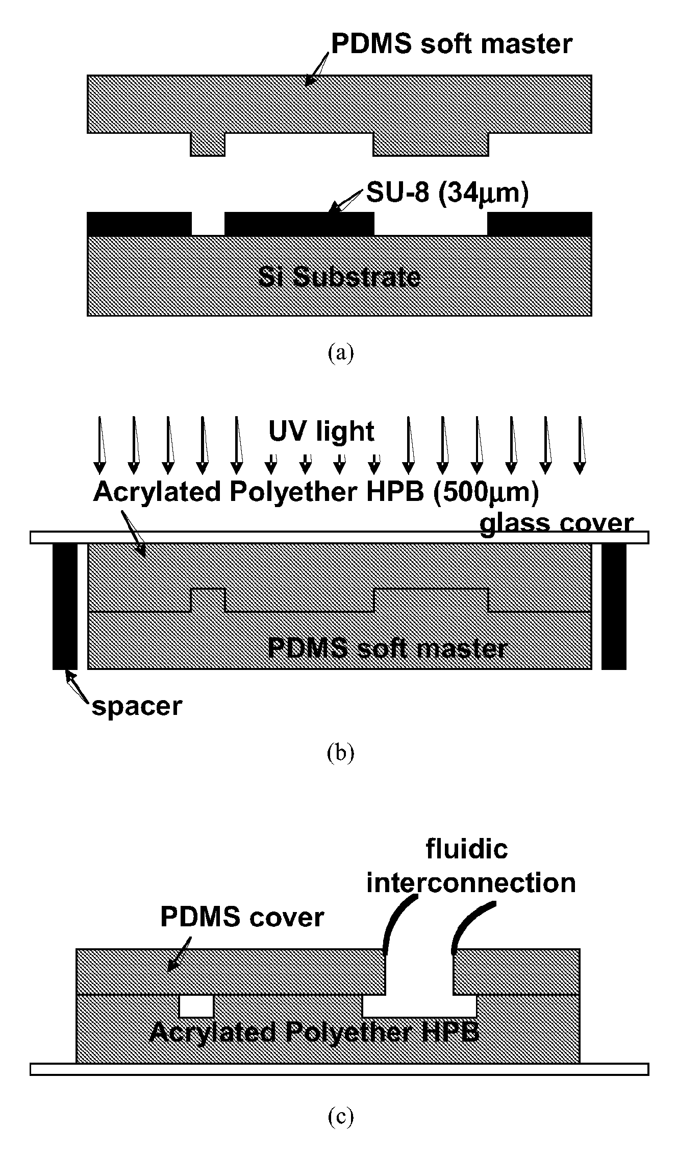
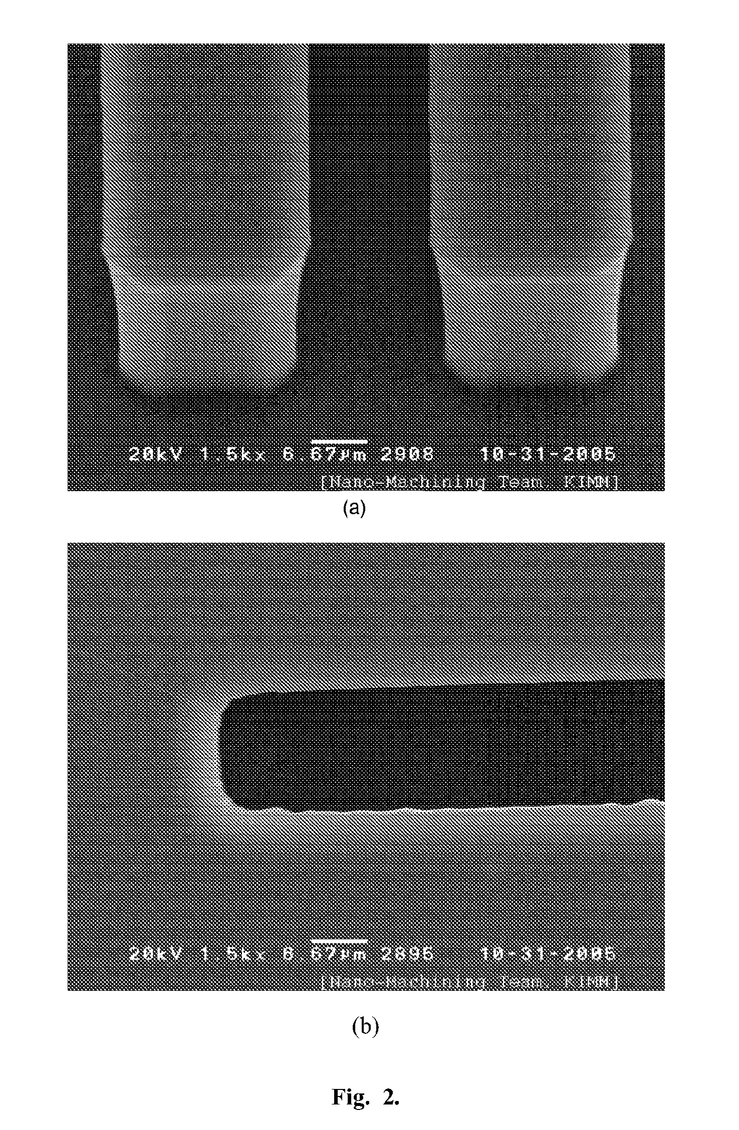
[0029]A fluidic digital-to-analog converter [25] was fabricated using the novel process (FIG. 1) with Acrylated Polyether HBP detailed in example 1. The microscopic view of the overall fabricated device is shown in FIG. 4a. The chip size was 1.5 mm×1.5 mm and it consists of four inlet ports, one outlet port and four microchannel networks. FIG. 4b shows the microscopic view of a microchannel network. The length of the microchannel is measured as 605.6±3.2 μm. SEM images of the microchannel cross-section are shown in FIG. 5. We compare designed and fabricated dimensions of the microchannel in Table 2. The error in slope angle, 6.6°, results from the PDMS master fabrication step. We observe the SU-8 pattern for the PDMS master (FIG. 1a) has a similar slop angle. Because of the slope angle, the top and bottom part of the microchannel have different widths, measured as 15.44±0.88 μm and 22.67±1.43 μm, respectively (Table 2). A fluidic filling test was c...


PUM

PropertyMeasurementUnit
temperatureaaaaaaaaaa
pressureaaaaaaaaaa

Abstract

The invention relates to novel polymer-based microstructures, with outstanding shape accuracy and cost-effective processing. The novel polymers are based on hyperbranched macromolecules and enable remarkable property combination such as reduced shrinkage and associated low stress, high shape fidelity and high aspect ratio in patterned microstructures, with additional benefit of fast and low-cost production methods. The invention also relates to methods to produce these microstructures. The polymer-based microstructures are relevant for, but not limited to micro- and nano- technologies applications, including lab-on-a-chip devices, opto-electronic and micro- electromechanical devices, optical detection methods, in fields of use as diverse as automotive, aerospace, information technologies, medical and biotechnologies, and energy systems.

Description

FIELD OF THE INVENTION[0001]The invention relates to micro devices such as microfluidic devices which are at least partially made of polymers.BACKGROUND OF THE INVENTION[0002]The term hyperbranched polymers (HBP) used herein refers to dendrimers, hyperbranched macromolecules and other dendron-based architectures and derivatives of all of them, and their reactive blends with multifunctional polymers.[0003]The term “micro” used herein indifferently refers to applications and objects having a micrometer or nanometer scale.[0004]Polymers offer numerous advantages for microfluidic applications, like ease of fabrication, using replication process, and biocompatibility. Polymer-based devices are cheap enough to be disposable. Polymer materials such as polycarbonate, polyimide, polymethylmethacrylate, polydimethylsiloxane (PDMS), and cyclic olefin copolymer (COC) have been explored for micro devices. See for example international patent application WO 2004 / 007582. Among them, PDMS and COC a...

Claims


Application Information

Patent Timeline
Patent Type & Authority Applications(United States)
IPC IPC(8): B01J19/00C08F2/48
CPCB81C1/00634C08L101/005C08G83/005C08G83/002B81B1/00C08G65/32C08G83/00C08L101/00
Inventor SCHMIDT, LARSLETERRIER, YVESMANSON, JAN-ANDERSCHO, YOUNG-HOJIN, YOUNG-HYUN
Owner KOREA ADVANCED INST OF SCI & TECH
Why Eureka
Try Eureka