

Semiconductor device
a technology of semiconductor devices and semiconductors, applied in the direction of antennas, antenna details, antenna feed intermediates, etc., can solve the problems of easy peeling of copper plating layers from substrates, adverse effects easy so as to reduce the adverse effect of copper diffusion on electrical characteristics of circuit elements, improve adhesion, and reduce the peeling of copper plating layers
- Summary
- Abstract
- Description
- Claims
- Application Information
AI Technical Summary
Benefits of technology
Problems solved by technology
Method used
Image

Examples
embodiment mode 1
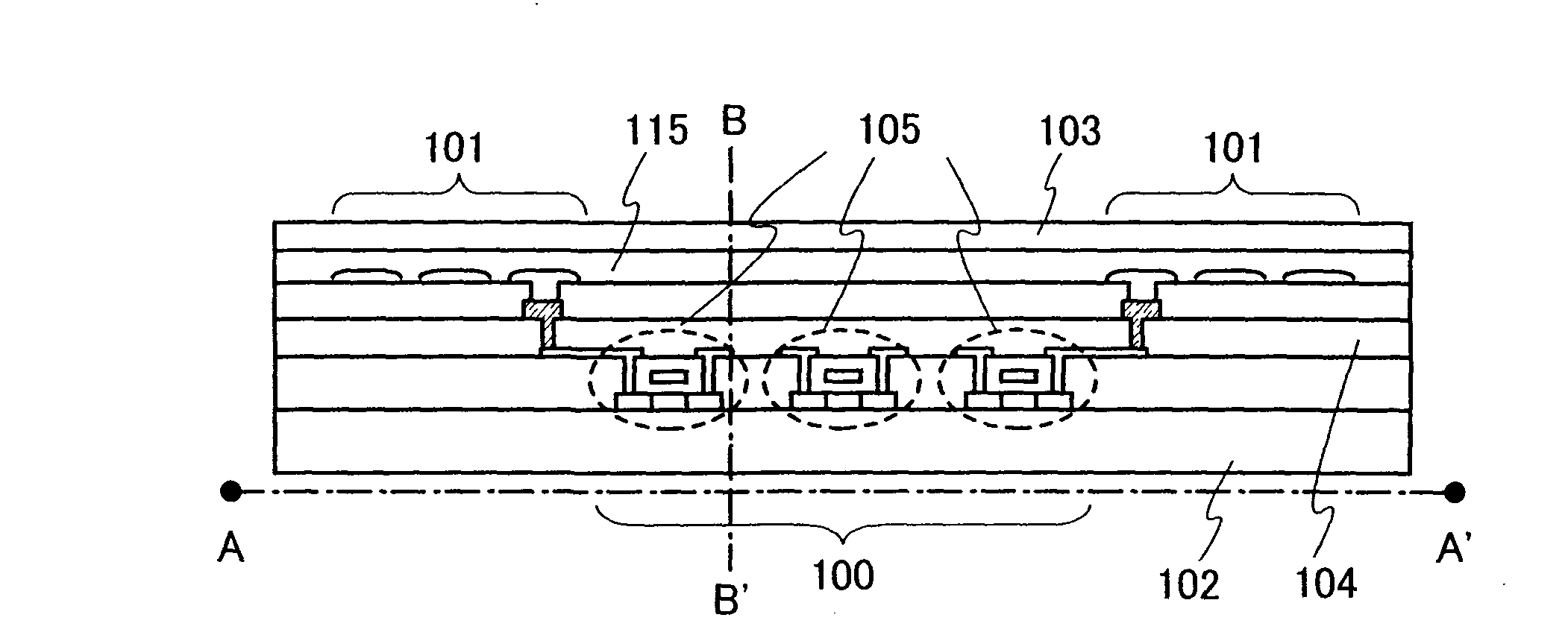
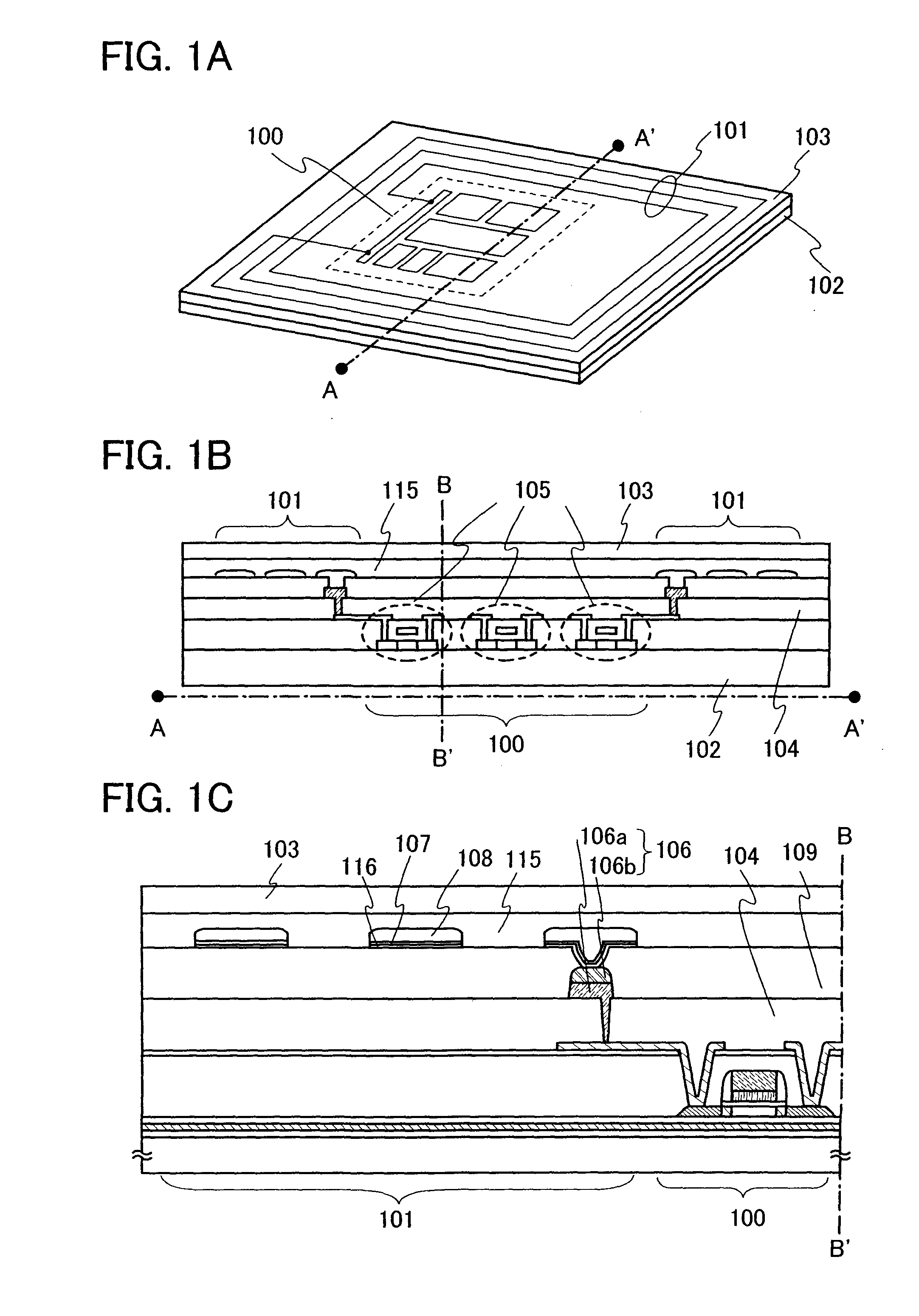
[0028]Embodiment Mode 1 of a semiconductor device of the present invention will hereinafter be described with reference to drawings. FIGS. 1A to 1C show a wireless chip as an example of a semiconductor device of the present invention. FIG. 1A is a perspective view of the wireless chip, FIG. 1B is a cross sectional view thereof along A-A′ of FIG. 1A, and FIG. 1C is a magnified view of a left part from a chain line B-B′ of FIG. 1B.
[0029]In FIG. 1A, an integrated circuit 100 and an antenna 101 are formed over one substrate 102 and covered by a cover member 103. A planar shape of the antenna 101 has a rectangular and spiral shape, and the antenna 101 is electrically connected to the integrated circuit 100.
[0030]In FIG. 1B, the integrated circuit 100 is formed over the substrate 102 and the antenna 101 is formed over a third interlayer insulating film 104 that covers the integrated circuit 100. A protection film 115 and the cover member 103 are formed over the antenna 101.
[0031]Although ...
embodiment mode 2
[0064]Next, an example of a circuit configuration of the wireless chip described in Embodiment Mode 1 is shown. FIG. 4 is a block diagram for illustrating circuits of the wireless chip.
[0065]FIG. 4 shows an example of a block diagram of a circuit arrangement of the wireless chip of the present invention. In FIG. 4, a reader / writer 401 is a device for writing and reading data in and from a wireless chip 400 from outside without contact. The wireless chip 400 includes an antenna portion 402 for receiving electromagnetic waves; a rectifier circuit 403 for rectifying the output of the antenna portion 402; a regulator circuit 404 for outputting operating voltage VDD to each circuit upon the receipt of the output from the rectifier circuit 403; a clock generator circuit 405 for generating clock upon the receipt of the output from the regulator circuit 404; a booster circuit 407 for supplying data-writing voltage to a memory circuit 408 that carries out data writing or reading, upon the re...
embodiment mode 3
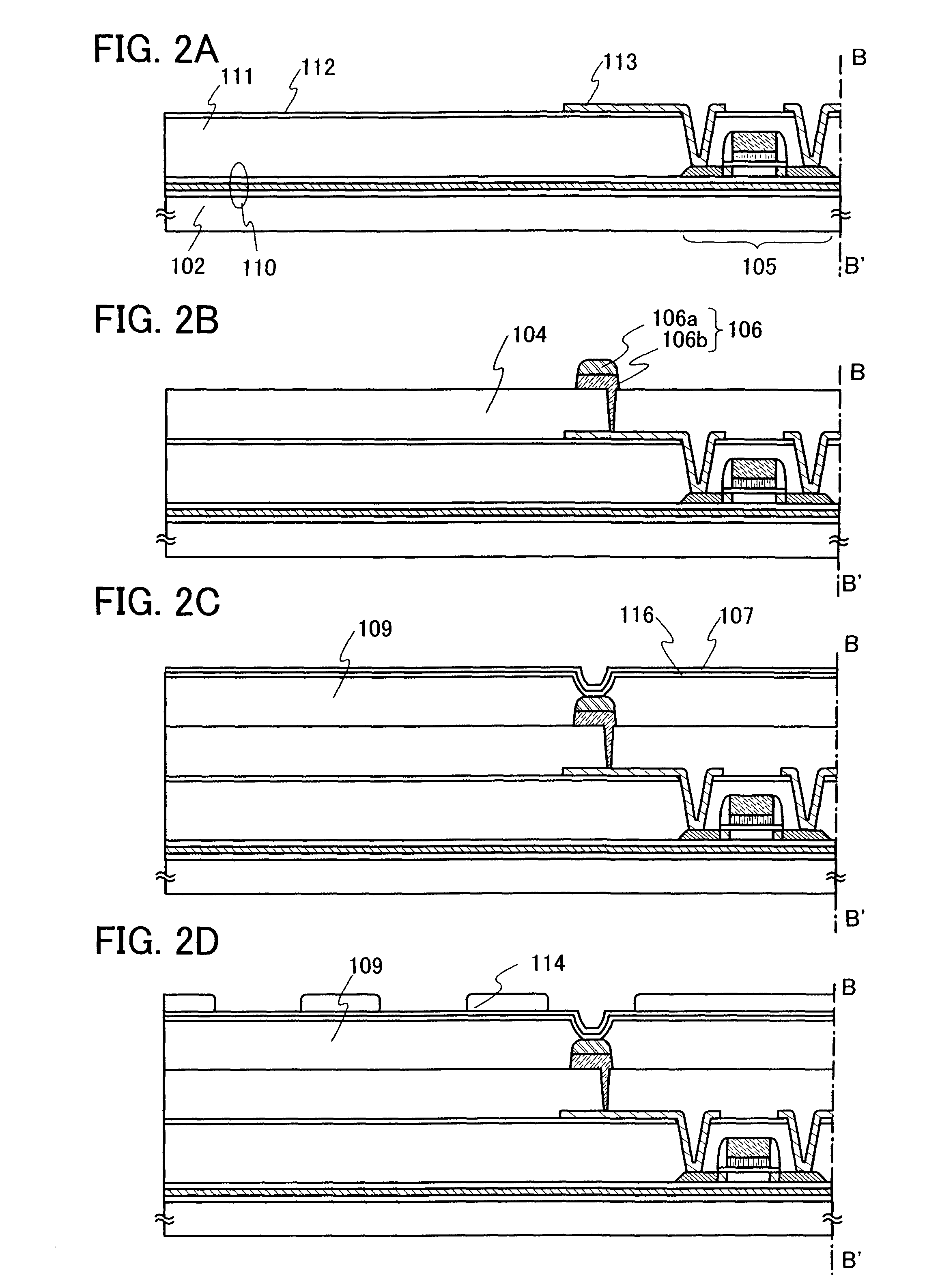
[0076]Next, a method of manufacturing a wireless chip of another embodiment mode of the present invention will be explained in detail. Although this embodiment mode shows a TFT as an example of a semiconductor element used for an integrated circuit of a wireless chip, a semiconductor element used for an integrated circuit is not limited to this, and any kind of semiconductor element can be used.
[0077]First, a release layer 501 is formed over a heat-resistant first substrate 500 as shown in FIG. 5A. The first substrate 500 may be, for example, a glass substrate such as a barium borosilicate glass substrate or an aluminoborosilicate glass substrate, a quartz substrate, a ceramic substrate, or the like. Moreover, the first substrate 500 may be a semiconductor substrate or a metal substrate including a stainless steel substrate. A substrate formed of a synthetic resin having flexibility, such as plastic, generally tends to have lower allowable temperature limit than the above-described ...
PUM
 Abstract
Description
Claims
Application Information