Method of Forming a Self Aligned Copper Capping Layer

a self-aligning, copper capping technology, applied in the direction of semiconductor devices, semiconductor/solid-state device details, electrical apparatus, etc., to achieve the effect of preventing further indiffusion thereof, preventing inter-metal line leakage, and improving adhesion

Inactive Publication Date: 2008-12-18
NXP BV
View PDF9 Cites 49 Cited by
  • Summary
  • Abstract
  • Description
  • Claims
  • Application Information

AI Technical Summary

Benefits of technology

[0024]In a first exemplary embodiment of the invention, the interconnect line and layer of said second metal is subjected to a reactive annealing process in an environment containing said non-metallic substance, so as to cause indiffusion of atoms of the second metal into the interconnect line and create an alloyed layer at the surface of the interconnect line, which alloyed layer reacts with the atoms of the non-metallic substance to form the diffusion barrier. The reaction with the atoms of the non-metallic substance to form the above-mentioned compound has the advantage of pinning the second metal in the matrix of the first metal (to prevent further indiffusion thereof into the interconnect line). The reactive atmosphere during the annealing process may typically comprise N2/H2, NH3, or N2) plasma or a furnace anneal in an ammonia environment. In the case where the layer of said second metal is deposited additionally on the surface of the dielectric layer, the reaction with the atoms of the non-metallic substance causes the portions of the layer of second metal on the dielectric to be transformed to an insulative compound of said second metal, which has the additional advantage of preventing inter-metal line leakage. This insulative compound may (optionally) be subsequently removed by, for example, wet chemical or etch stripping means (e.g. chloride based chemistries). However, if it is not removed, it can act as a ...

Problems solved by technology

Furthermore, Al and Mg are soluble in copper to a relatively sm...

Method used


Image

  • Method of Forming a Self Aligned Copper Capping Layer
  • Method of Forming a Self Aligned Copper Capping Layer
  • Method of Forming a Self Aligned Copper Capping Layer

Examples


Embodiment Construction

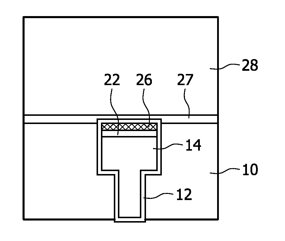
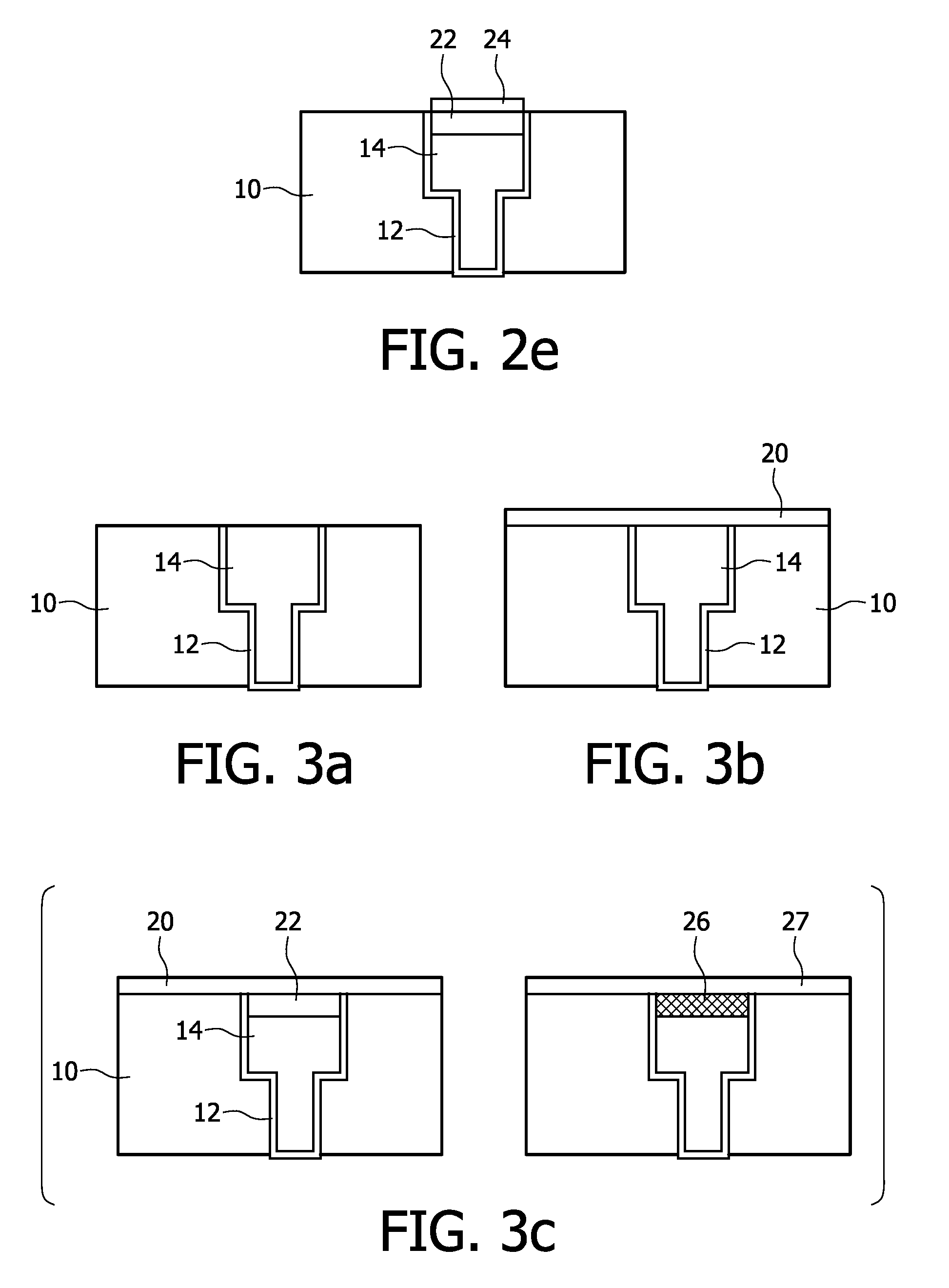
[0035]A process is thus proposed herein for the formation of a self-aligned Cu-alloy capping layer on a metal interconnection that has improved adhesion properties and resistance to electromigration and stress-induced voiding near the upper part of the interconnect lines. This is achieved by forming an intermetallic compound, for example, a copper alloyed compound (e.g. CuAlN) near the top of the interconnect lines. Thus, the indiffusion of aluminium into the copper can be controlled.

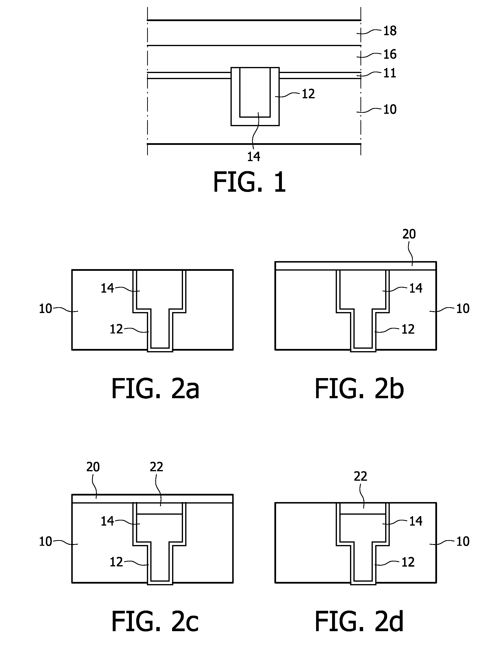
[0036]Starting from the structure following the Chemical Mechanical Polishing step, and referring to FIGS. 3a and 4a of the drawings, a copper interconnect 14 is embedded within a intrametal dielectric layer 10 with a barrier layer 12 therebetween. In a first exemplary embodiment of the present invention, a thin metallic Al (or Mg, B, Zn, etc) film 20 is deposited on top of the metal lines 14 and dielectric layer 10 by, for example, PVD, CVD or ALD, as illustrated in FIG. 3b. Next, and as illustrated in...


PUM


Abstract

A method of forming a capping layer on a copper interconnect line (14). The method comprises providing a layer (20) of Aluminium over the interconnect line (14) and the dielectric layer (10) in which it is embedded. This may be achieved by deposition or chemical exposure. The structure is then subjected to a process, such as annealing or further chemical exposure, in an environment containing, for example, Nitrogen atoms, so as to cause indiffusion of Al into the copper line (14) and nitridation to form a diffusion barrier 26 of the intermetallic compound CuAlN.

Description

FIELD OF THE INVENTION[0001]The invention relates to a method of forming a self-aligned copper capping layer in respect of a copper interconnect layer of a semiconductor device, so as to improve the reliability thereof and to improve capacitive coupling between the lines.BACKGROUND OF THE INVENTION[0002]Aluminium has, in the past, been the principal conductive material employed for electrical interconnection in semiconductor devices due to its low resistivity, good adherence to silicon dioxide, low cost, ease in bonding and good etchability. As device geometry continues to scale down for Ultra Large Scale Integrated circuits, there is a growing demand for an interconnect wiring with minimum pitch and high conductivity, while requiring greater levels of reliability. Currently, an integrated circuit is considered good if a test indicates an equivalent life span of 10 years. However, in some specific applications, such as space (e.g. satellite, probe, etc), medical (e.g. pacemakers and...

Claims


Application Information

Patent Timeline
IPC IPC(8): H01L21/4763
CPCH01L21/76834H01L21/76849H01L21/76856H01L21/76867H01L21/76886H01L23/53238H01L2924/0002H01L23/53295H01L2924/3011H01L2924/00H01L21/28H01L21/768H01L23/522
Inventor BESLING, WIMVANYPRE, THOMAS
Owner NXP BV
Why Eureka
Try Eureka