Differential transmitter, differential receiver, signal transmitter, and signal transmitting system

Inactive Publication Date: 2009-02-26
RENESAS ELECTRONICS CORP
View PDF5 Cites 11 Cited by
  • Summary
  • Abstract
  • Description
  • Claims
  • Application Information

AI Technical Summary

Benefits of technology

[0027]According to the technique of the present invention, it is possible to reduce

Problems solved by technology

When such an MPU is employed in an information processing device or especially a server/workstation, high-speed and large amount of data transmission is needed.
In this case, the receiving side (differential receiver block 30 side) may respond to small potential difference due to the influence of the noise in the actual operation and may accidentally receive the sig

Method used


Image

  • Differential transmitter, differential receiver, signal transmitter, and signal transmitting system
  • Differential transmitter, differential receiver, signal transmitter, and signal transmitting system
  • Differential transmitter, differential receiver, signal transmitter, and signal transmitting system

Examples


Example

First Embodiment

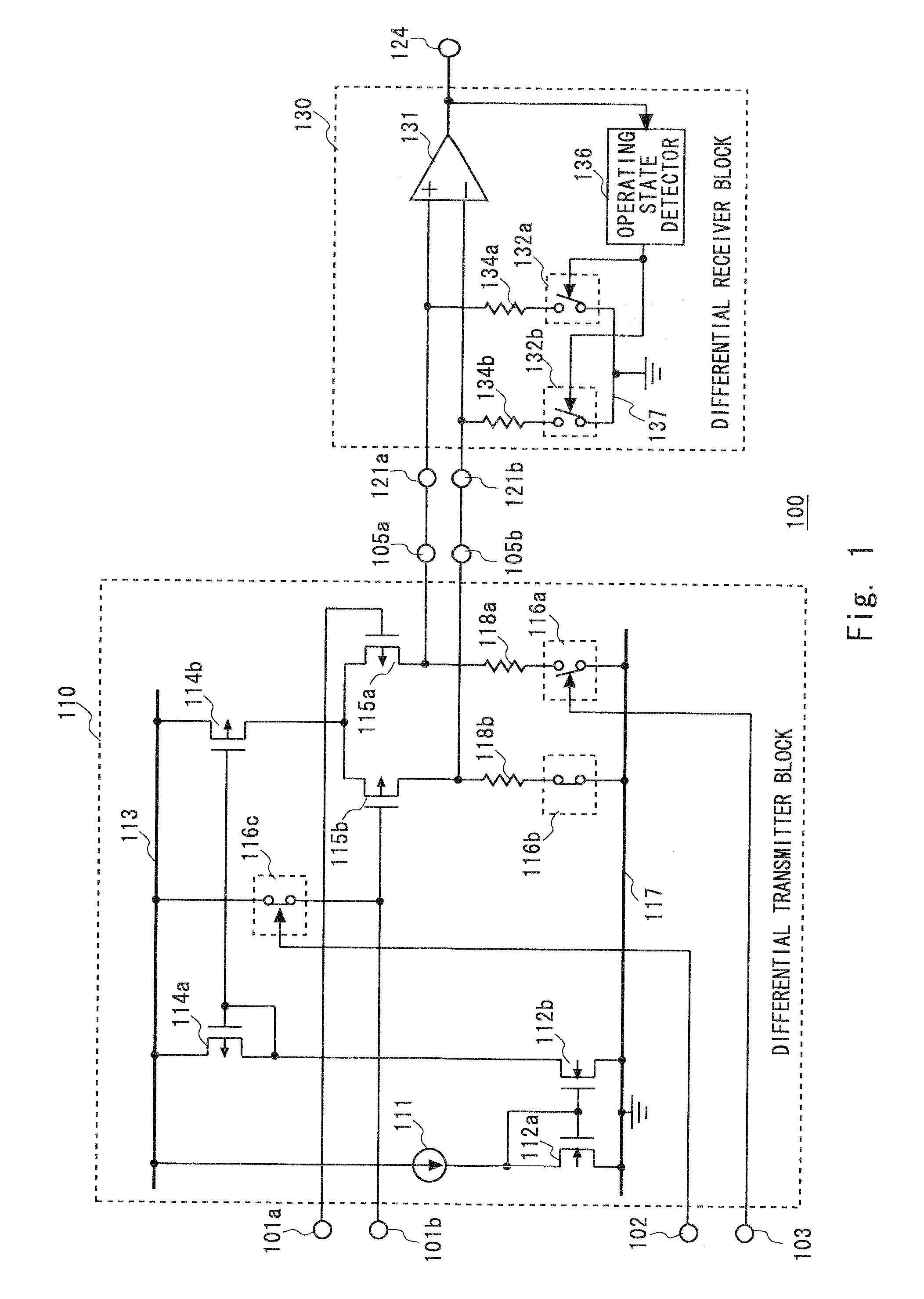
[0040]FIG. 1 shows a differential transceiver 100 according to the first embodiment of the present invention. The differential transceiver 100 includes a differential transmitter block 110 in a current driver side, and a differential receiver block 130.

[0041]The differential transmitter block 110 includes a constant current source 111, N transistors 112a and 112b receiving a constant current from the constant current source 111 to form a mirror circuit, P transistors 114a and 114b connected to a power line 113 to form a constant current source, P transistors 115a and 115b functioning as switches for logic output, and terminating resistors 118a and 118b connected to a ground line 117. Further, there is a switch 116a provided between the terminating resistor 118a and the ground line 117. On / Off of the switch 116a is controlled by a control signal from a control terminal 103. Additionally, there is a switch 116b provided between the terminating resistor 118b and the gro...

Example

Second Embodiment

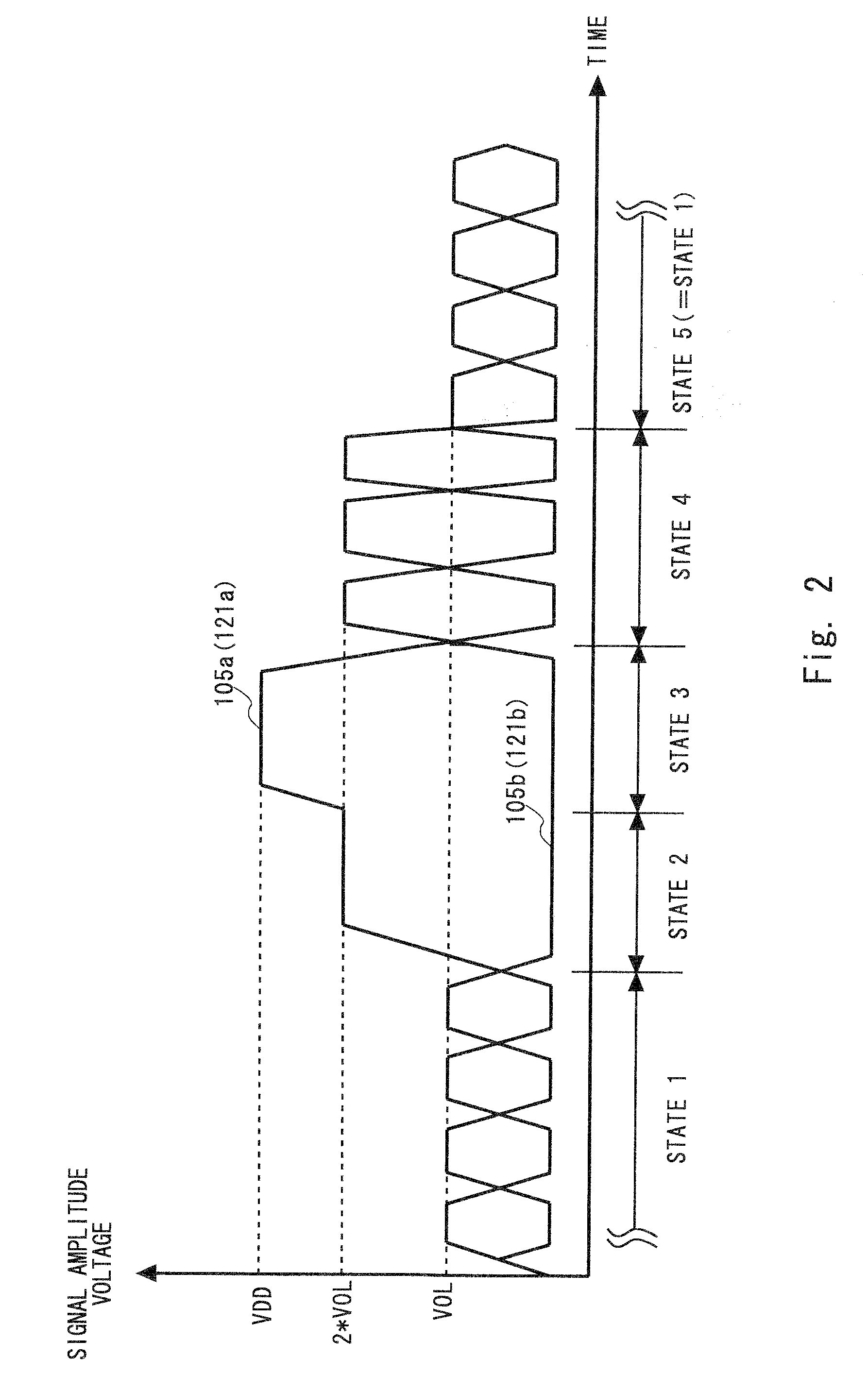
[0063]FIG. 4 shows a differential transceiver 200 according to the second embodiment of the present invention. The differential transceiver 200 specifically shows the details of the operating state detector 136 and switches of the differential transceiver 100 of the first embodiment. In FIG. 4, the same components as those of the differential transceiver 100 are denoted by the same reference symbols except the operating state detector 136 and switches, and the overlapping description thereof will be omitted. Further, the differential transceiver 200 shown in FIG. 4 can also assume five states of state 1 to state 5 as in the same way as the differential transceiver 100 shown in FIG. 1.

[0064]As shown in FIG. 4, in the differential transmitter block 210 of the differential transceiver 200, an N transistor 216a is provided between the terminating resistor 118a and the ground line 117, an N transistor 216b is provided between the terminating resistor 118b and the ground ...

Example

Third Embodiment

[0077]FIG. 5 is a differential transceiver 300 according to the third embodiment of the present invention. In the differential transceiver 300, the terminating resistors and the switches connected thereto are integrated with respect to the differential transceiver 200 shown in FIG. 4 based on the fact that the ON resistance of the transistor is determined by a design of a gate width and a gate length. Other functional components are the same as those of the differential transceiver 200 shown in FIG. 4 except for this point. Therefore, only the terminating resistors in the transmitting and receiving sides and the switches connected thereto are described regarding the differential transceiver 300.

[0078]In the differential transmitter block 310 of the differential transceiver 300, the N transistor 318a corresponds to the terminating resistor 118a and the N transistor 216a in the differential transmitter block 210 of the differential transceiver 200, and the N transistor...


PUM


Abstract

According to one embodiment of the present invention, it is possible to realize a signal transmitter which is capable of reducing power consumption and which can be easily designed. A differential transmitter block outputs differential output signals fixed to a predetermined logic signal to a differential receiver block and disconnects terminating resistors from a signal transmission path in an idle state. In the differential receiver block, a differential comparator outputs a logic determined by symbols of the differential output signal from the differential transmitter block, and an operating state detector detects the idle state upon detection that time successively outputting a predetermined logic by the differential comparator reaches a predetermined time, and controls switches so as to disconnect the terminating resistors from the signal transmitter in the receiving side upon detection of the idle state.

Description

BACKGROUND OF THE INVENTION[0001]1. Field of the Invention[0002]The present invention relates to a signal transmission, and more particularly, to a signal transmission technique by a differential input / output circuit.[0003]2. Description of Related Art[0004]Along with current advancement of an LSI (large-scale integrated circuit) manufacturing technique, a high-performance MPU (Micro Processor Unit) whose operating frequency exceeds 1 GHz has been developed. When such an MPU is employed in an information processing device or especially a server / workstation, high-speed and large amount of data transmission is needed. In order to achieve this, a system connecting the MPU with each module of a memory by PTP (Point-to-Point) employing an FB-DIMM (Fully Buffered Dual Inline Memory Module) has been used, for example. The FB-DIMM includes an AMB (Advanced Memory Buffer) chip for connection between modules mounted thereon in addition to a memory chip, and employs high-speed serial interface...

Claims


Application Information

Patent Timeline
IPC IPC(8): H04B3/00
CPCH04L25/0272H04L25/0292H04L25/029H03K17/00
Inventor IWASAKI, TADASHI
Owner RENESAS ELECTRONICS CORP
Why Eureka
Try Eureka