Field-Effect Semiconductor Device, and Method of Fabrication

a field-effect semiconductor and semiconductor technology, applied in semiconductor devices, semiconductor/solid-state device details, electrical apparatus, etc., can solve the problems of easy noise triggering, inconvenient use of conventional normally-on hemts, and unnecessary associated circuitry, so as to prevent current collapse, reduce current leakage, and save the two-dimensional carrier gas layer

Active Publication Date: 2009-03-05
SANKEN ELECTRIC CO LTD
View PDF2 Cites 122 Cited by
  • Summary
  • Abstract
  • Description
  • Claims
  • Application Information

AI Technical Summary

Benefits of technology

[0030]In still another embodiment the main semiconductor region has a fourth semiconductor layer (e.g., third electron supply layer) on the third semiconductor layer. Of a nitride semiconductor with an aluminum proportion less than that of the third semiconductor layer (e.g., second electron supply layer), the fourth semiconductor layer is effective to electrically stabilize the surface of the main semiconductor region, reducing current leakage and preventing current collapse.
[0031]In a further embodiment the main semiconductor region has a fifth semiconductor layer of a nitride semiconductor with an aluminum proportion less than that of the underlying fourth semiconductor layer. Doped into a conductivity type (e.g., n-type) opposite to that of the metal oxide semiconductor film, the fifth semiconductor layer serves for better ohmic contact with the overlying two main electrodes.
[0032]The main semiconductor region may additionally comprise a spacer between the first and the second semiconductor layer, the spacer being thinner than the second semiconductor layer and containing aluminum in a higher proportion than the second semiconductor layer. The spacer functions to bar the diffusion of impurities or elements from the second into the first semiconductor layer and hence to save the two-dimensional carrier gas layer from a decline in the mobility of the charge carriers.
[0033]For surface stabilization of the main semiconductor film, an insulating film may be employed which covers at least parts of the major surface of the main semiconductor region between the first main electrode and the gate electrode and between the second main electrode and the gate electrode. Additionally, made from a silicon oxide in particular, the insulating film will develop a compressive stress of, say, 4.00×10⁹ dyn / cm2. Caused by this compressive stress, the piezoelectric depolarization of the second semiconductor layer of the main semiconductor region will lead to a higher density of the charge carriers (e.g., electrons) in the two-dimensional carrier gas layer (e.g., 2DEG layer). The turn-on resistance of the device will then be less than in the prior art case where a silicon nitride film, rather than the silicon oxide film above, was provided on the major surface of the main semiconductor region.
[0034]Use of a gate field plate is recommended for mitigation of field concentrations. Disposed on the major surface of the main semiconductor region via the insulating film and coupled to the gate electrode, the gate field plate will serve the additional purpose of permitting the electrons that have been trapped at the surface states of the main semiconductor region to be drawn therethrough when a high voltage is applied to the device, thereby saving the same from current collapse and preventing a rise in turn-on resistance.
[0035]The insulating film may be formed to include slanting side surfaces underlying the field plate. Field concentrations at the edges of the gate electrode will then diminish, enabling the device to withstand higher voltages.

Problems solved by technology

Use of such a negative power supply made the associated circuitry unnecessary complex and expensive.
The conventional normally-on HEMTs were rather inconvenient of use.
However, the HEMT built on this known scheme had a threshold voltage as low as one volt or even less and so was easy to be triggered into action by noise.
What was worse, this threshold changed substantively with manufacturing errors in the depth of the recess in the electron supply layer.
Another weakness was that there was a relatively large current leakage upon application of a positive voltage to the Schottky gate.
Creating the recess in the electron supply layer brought about an additional shortcoming that the resulting thin part of the electron supply layer became incapable of supplying a sufficient amount of electrons to the electron transit layer even when a voltage was applied to the gate in order to turn the device on.
The fact that the 2DEG layer was partly insufficient in electron density the turn-on resistance of the device inordinately high.
The resulting depletion of electrons from under the gate creates a hiatus in the 2DEG layer, making the device normally off.
An objection to this second known suggestion is the difficulty of creating the p-type nitride semiconductor layer of the sufficiently high hole density required.
As an additional disadvantage, the insulating film was susceptible to physical defects, particularly when made thinner for a higher transconductance.
A defective insulating film was a frequent cause of current leakage, lower antivoltage strength, device destruction, and current collapse.
All these results would be avoidable by making the insulating film thicker, but then the device would be inconveniently low in transconductance.
A problem with this prior art device arose when the gate was excited to turn it on.
Similar problems have attended the conventional endeavors to provide other types of normally-off field-effect semiconductor devices such as MESFETs and 2DEG diodes.

Method used


Image

  • Field-Effect Semiconductor Device, and Method of Fabrication
  • Field-Effect Semiconductor Device, and Method of Fabrication
  • Field-Effect Semiconductor Device, and Method of Fabrication

Examples


embodiment

of FIG. 7

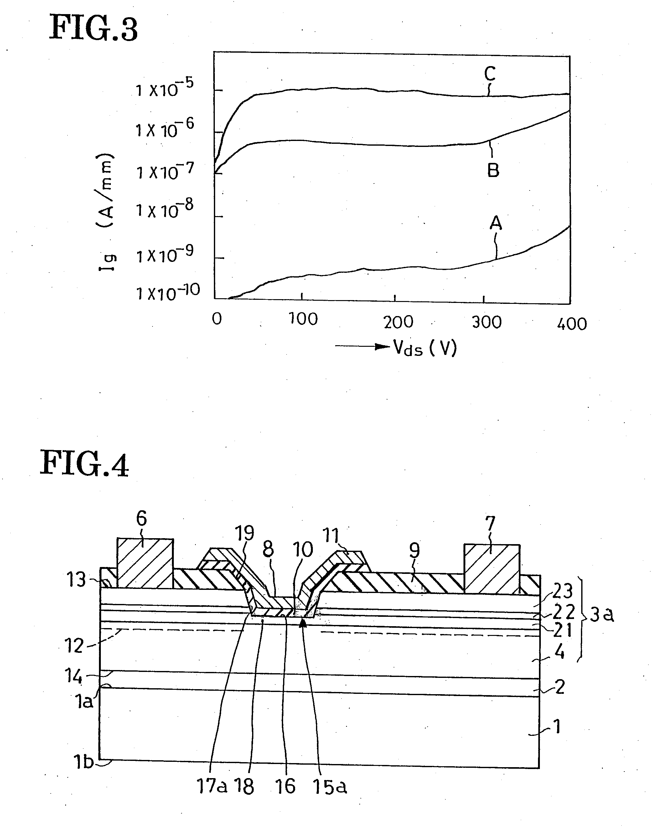
[0139]This embodiment is akin to that of FIG. 4 except for the main semiconductor region 3b. This main semiconductor region 3b, then, is similar to its FIG. 4 counterpart 3a except for the absence of the third electron supply layer 23, having the remaining two electron supply layers 21 and 22′ deposited one after the other on the electron transit layer 4. The first electron supply layer 21 is of the same make as that indicated by the same numeral in FIG. 4. The second electron supply layer 22′ is the same as its FIG. 4 counterpart except being thicker, being 10-150 nanometers, preferably about 18 nanometers, thick.

[0140]Having the two electron supply layers 21 and 22′ of the same compositions as their FIG. 4 counterparts 21 and 22, this embodiment possesses the same benefits as does that of FIG. 4 except those accruing from the third electron supply layer 23. The material of the second electron supply layer 22′ is alterable into a semiconducting nitride not doped with silic...


PUM


Abstract

A HEMT-type field-effect semiconductor device has a main semiconductor region comprising two layers of dissimilar materials such that a two-dimensional electron gas layer is generated along the heterojunction between the two layers. A source and a drain electrode are placed in spaced positions on a major surface of the main semiconductor region. Between these electrodes, a gate electrode is received in a recess in the major surface of the main semiconductor region via a p-type metal oxide semiconductor film whereby a depletion zone is normally created in the electron gas layer, with a minimum of turn-on resistance and gate leak current.

Description

CROSS REFERENCE TO RELATED APPLICATIONS[0001]This application claims priority to Japanese Patent Application No. 2007-222273, filed Aug. 29, 2007, and Japanese Patent Application No. 2008-073603 filed Mar. 21, 2008.BACKGROUND OF THE INVENTION[0002]This invention relates to semiconductor devices, particularly to field-effect semiconductor devices as typified by the high electron mobility transistor (HEMT), the two-dimensional electron gas (2DEG) diode (diode that utilizes a layer of 2DEG as a current path or channel), and the metal-semiconductor field-effect transistor (MESFET). More particularly, the invention pertains to such field-effect semiconductor devices that are normally off, instead of normally on as in the case of most of such devices known heretofore. The invention also deals with a method of fabricating such normally-off field-effect semiconductor devices.[0003]The HEMT has been known and used extensively which comprises an electron transit layer of undoped semiconductin...

Claims


Application Information

Patent Timeline
Patent Type & Authority Applications(United States)
IPC IPC(8): H01L29/778
CPCH01L29/42316H01L29/808H01L29/7787H01L29/432H01L29/2003
Inventor KANEKO, NOBUO
Owner SANKEN ELECTRIC CO LTD
Why Eureka
Try Eureka