Semiconductor device and electronic appliance

a technology of semiconductor devices and electronic appliances, applied in the direction of semiconductor devices, basic electric elements, electrical appliances, etc., can solve the problems of low heat resistance of semiconductor devices, temperature limitation to 700°, and inability to heat at temperatures, etc., and achieve the effect of expanding the area

Inactive Publication Date: 2009-03-19
SEMICON ENERGY LAB CO LTD
View PDF33 Cites 33 Cited by
  • Summary
  • Abstract
  • Description
  • Claims
  • Application Information

AI Technical Summary

Benefits of technology

[0007]Glass substrates are larger in area and more inexpensive than silicon wafers, and are mainly used for manufacturing display devices su...

Problems solved by technology

However, the strain point of a glass substrate is equal to or lower than 700° C., and the heat resistance thereof is low.
Therefore, heating cannot be performed at temperatures over the allowable temperature limit of the glass substrate and the process temperature is limited to 700° C. or below.
That is, there is limitation of process temperature also in removing a crystal defect or surface roughness in the separation plane.
Further, there is limitation of process temperature also in manufacturing a transistor with the use of a single-crystal-silicon layer attached to a glass substrate.
F...

Method used


Image

  • Semiconductor device and electronic appliance
  • Semiconductor device and electronic appliance
  • Semiconductor device and electronic appliance

Examples


embodiment mode 1

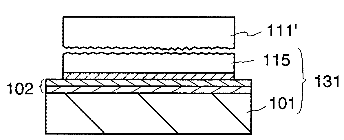
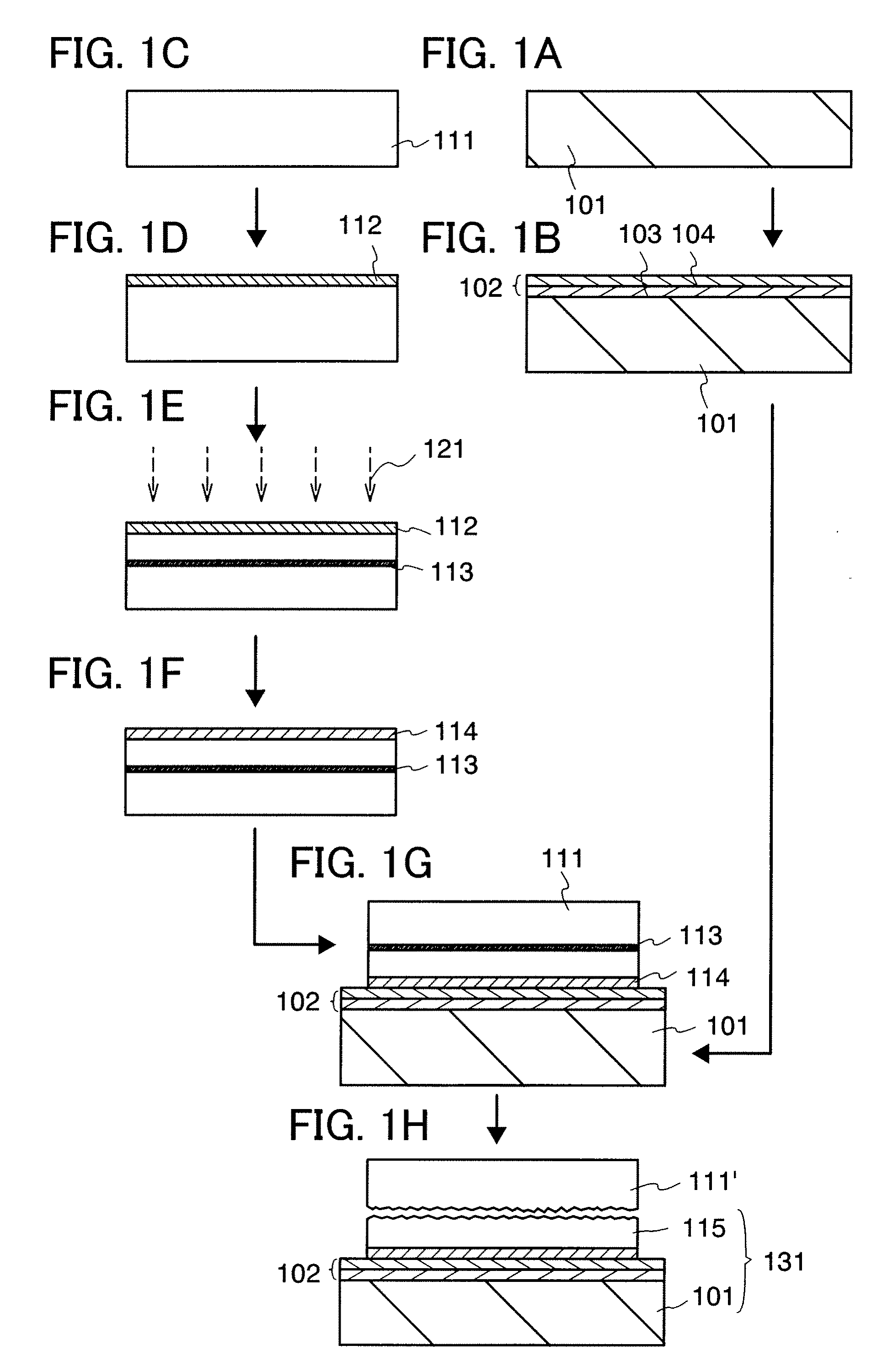
[0057]FIGS. 1A to 1H and FIGS. 2A to 2C are cross-sectional views showing an example of a method for manufacturing an SOI substrate used for a semiconductor device of the present invention. An example of a method for manufacturing an SOI substrate will be described below using FIGS. 1A to 1H and FIGS. 2A to 2C.

[0058]First, a base substrate 101 is prepared (see FIG. 1A). As the base substrate 101, a light-transmitting glass substrate which is used for an electronic product such as a liquid crystal display device can be used. It is preferable to use, as the glass substrate, a substrate having a coefficient of thermal expansion which is greater than or equal to 2.5×10⁻⁶ / ° C. and less than or equal to 5.0×10⁻⁶ / ° C. (preferably, greater than or equal to 3.0×10⁻⁶ / ° C. and less than or equal to 4.0×10⁻⁶ / ° C.) and a strain point which is equal to or higher than 580° C. and equal to or lower than 680° C. (preferably, equal to or higher than 600° C. and equal to or lower than 680° C.) in term...

embodiment mode 2

[0150]FIGS. 5A to 5H and FIGS. 6A to 6C are cross-sectional views showing another example of the method for manufacturing an SOI substrate used for the semiconductor device of the present invention. Another example of the method for manufacturing an SOI substrate will be described below using FIGS. 5A to 5H and FIGS. 6A to 6C.

[0151]As described in Embodiment mode 1 using FIG. 1A, the base substrate 101 which serves as a base substrate of an SOI substrate is prepared (see FIG. 5A), and the insulating layer 102 is formed over the base substrate 101. Also in this embodiment mode, the insulating layer 102 is a two-layer film of the silicon nitride oxide film 103 and the silicon oxynitride film 104. Next, a bonding layer 105 is formed over the insulating layer 102 (see FIG. 5B). This bonding layer 105 can be formed in a similar manner to the bonding layer 114 formed over the semiconductor substrate 111, described in Embodiment Mode 1 or 2.

[0152]FIGS. 5C to 5E show the same process as sho...

embodiment mode 4

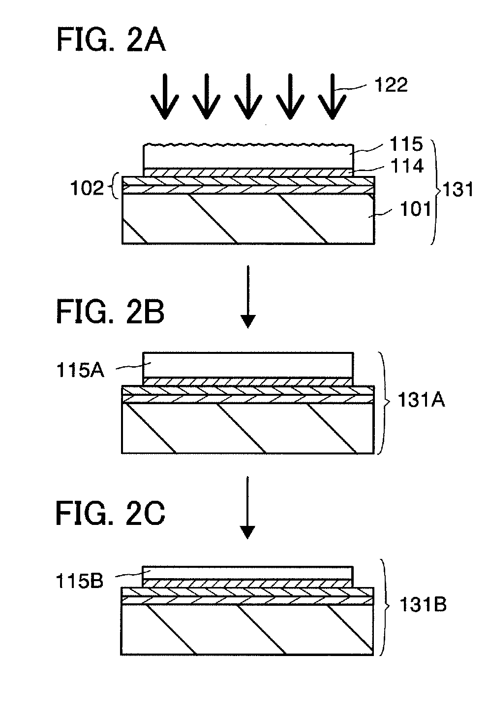
[0166]In each of Embodiment Modes 1 to 3, before the irradiation of the semiconductor layer 115 with the laser beam 122, a thinning step in which the semiconductor layer 115 is thinned by etching treatment (or etch-back treatment) can be performed. In the case of using an ion doping apparatus for the formation of the embrittlement layer 113, it is difficult to control the thickness of the semiconductor layer 115 to less than or equal to 100 nm. Therefore, the semiconductor layer 115 just after the separation is relatively thick. When the semiconductor layer 115 is thick, the irradiation energy density of the laser beam 122 needs to be high, and accordingly, the applicable range of the irradiation energy density becomes narrower, and it becomes difficult to planarize the semiconductor layer 115 and recover crystallinity of the semiconductor layer 115 with high yield by irradiation with the laser beam 122.

[0167]Therefore, when the thickness of the semiconductor layer 115 exceeds 200 n...


PUM


Abstract

A high-performance semiconductor device using an SOI substrate in which a low-heat-resistance substrate is used as a base substrate. Further, a high-performance semiconductor device formed without using chemical polishing. Further, an electronic device using the semiconductor device. An insulating layer over an insulating substrate, a bonding layer over the insulating layer, and a single-crystal semiconductor layer over the bonding layer are included, and the arithmetic-mean roughness of roughness in an upper surface of the single-crystal semiconductor layer is greater than or equal to 1 nm and less than or equal to 7 nm. Alternatively, the root-mean-square roughness of the roughness may be greater than or equal to 1 nm and less than or equal to 10 nm. Alternatively, a maximum difference in height of the roughness may be greater than or equal to 5 nm and less than or equal to 250 nm.

Description

TECHNICAL FIELD[0001]The present invention relates to a semiconductor device and an electronic appliance.[0002]Note that a semiconductor device in this specification refers to all devices which can function by utilizing semiconductor characteristics, and electro-optical devices, semiconductor circuits, and electronic appliances are all included in the category of the semiconductor device.BACKGROUND ART[0003]In recent years, instead of a bulk silicon wafer, integrated circuits using an SOI (silicon on insulator) substrate have been developed. By utilizing characteristics of a thin single-crystal-silicon layer formed over an insulating layer, transistors formed in the integrated circuit can be electrically separated from each other completely. Further, each transistor can be formed as a fully-depleted transistor, and thus a semiconductor integrated circuit with high added value such as high integration, high speed driving, and low power consumption can be realized.[0004]As a method fo...

Claims


Application Information

Patent Timeline
IPC IPC(8): H01L29/00
CPCH01L21/2007H01L21/76254H01L21/84H01L27/1214H01L29/78654H01L29/4908H01L29/66772H01L29/78603H01L27/1266H01L29/34
Inventor OHNUMA, HIDETOIIKUBO, YOICHIYAMAMOTO, YOSHIAKIMAKINO, KENICHIROSHIMOMURA, AKIHISAHIGA, EIJIMIZOI, TATSUYANAGANO, YOJIISAKA, FUMITOKAKEHATA, TETSUYAYAMAZAKI, SHUNPEI
Owner SEMICON ENERGY LAB CO LTD
Why Eureka
Try Eureka