

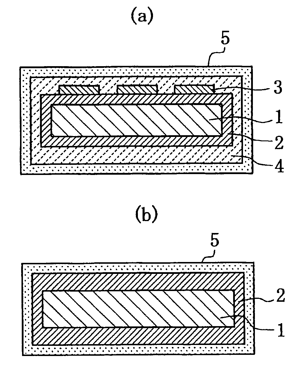
Electrostatic chuck member
a technology of electrostatic chuck and chuck member, which is applied in the direction of electrostatic holding device, basic electric elements, electric apparatus, etc., can solve the problems of inability to cool, complex structure of mechanical chuck, and inability to apply vacuum chuck to the recent production process of high-performance semiconductors, etc., to improve the semiconductor production system and enhance the etching effect and ra
- Summary
- Abstract
- Description
- Claims
- Application Information
AI Technical Summary
Benefits of technology
Problems solved by technology
Method used
Image

Examples
example 2
[0102]A coating is formed by spraying a coating material as shown in Table 3 onto a surface of an Al substrate having a size of 50 mm×100 mm×5 mm. Thereafter, a part of the coatings is subjected to an electron beam irradiation treatment to form a secondary recrystallized layer suitable for the invention. Then, a test specimen having a size of 20 mm×20 mm×5 mm is cut out from the resulting mass and masked so as to expose the surface of the irradiation treated coating at an area of 10 mm×10 mm and subjected to a plasma irradiation under the following conditions to measure a damaged quantity due to plasma erosion by means of an electron microscope or the like.[0103](1) Atmosphere Gas and Flow Rate Condition[0104]CF4 / Ar / O2=100 / 1000 / 10 ml (flow rate / min)[0105](2) Plasma Irradiation Output[0106]High frequency power: 1300 W[0107]Pressure: 133.3 Pa
[0108]The results are summarized in Table 3. As seen from the results of this table, all of anodized coating (No. 8), B4C spray coating (No. 9) a...
example 3
[0110]In this example, the coating is formed in the same manner as in Example 2 and then the resistance to plasma erosion of the coating is examined before and after the electron beam irradiation treatment. As a test specimen, a coating of the following mixed oxide is directly formed on an Al substrate at a thickness of 200 μm by an atmospheric plasma spraying method.[0111](1) 95% Y2O3-5% Sc2O3 [0112](2) 90% Y2O3-10% Ce2O3 [0113](3) 90% Y2O3-10% Eu2O3
[0114]Moreover, the electron beam irradiation after the formation of the coating, atmosphere gas component, plasma spraying conditions and the like are the same as in Example 2.
[0115]In Table 4 are summarized the results on the damaged quantity due to plasma erosion. As seen from the results, the oxides of Group 3A elements in the Periodic Table under conditions suitable for the invention (i.e. formation of densified re-melting layer by subjecting the surface of the spray coating to the electron beam irradiation) are good in the resist...
PUM
| Property | Measurement | Unit |
|---|---|---|
| roughness | aaaaa | aaaaa |
| thickness | aaaaa | aaaaa |
| electric resistivity | aaaaa | aaaaa |
Abstract
Description
Claims
Application Information