Semiconductor laser device and method for manufacturing the same

a laser device and semiconductor technology, applied in laser details, nanotechnology, nanooptics, etc., can solve the problems of aging cod level decline, failure mode generation, deterioration of the facet, etc., and achieve the effect of suppressing the cod level drop and high efficiency

Active Publication Date: 2009-04-02
PANNOVA SEMIC
View PDF6 Cites 14 Cited by
  • Summary
  • Abstract
  • Description
  • Claims
  • Application Information

AI Technical Summary

Benefits of technology

[0023]The present invention aims to provide a semiconductor laser device that is provided with high-output dual lasers formed monolithically and can suppress a decrease of a COD level during a high output operation of a laser, and a method for manufacturing the same.

Problems solved by technology

This failure mode is generated because a vicinity of the facet of the resonator of the semiconductor laser serves as a region for absorbing light that is generated inside the laser.
According to heat caused by nonradiative recombination via this deep level, the band gap is decreased further, thereby generating a positive feedback that causes more optical absorption, so that a temperature of the facet is increased steeply, which results in the deterioration of the facet due to its melting.
However, the prior arts as described in the above patent documents have a problem of decreasing the COD level during aging in high-output dual wavelength lasers including an AlGaAs infrared laser and an AlGaInP red laser that are formed monolithically on the same substrate.
However, in the case of forming the nitride semiconductor layer that functions also as the window structure, a lattice mismatch between a semiconductor layer and a nitride semiconductor layer of a gain region becomes large, which causes a large distortion of the facet.
It is considered that, if continuing aging in this state, a defect caused by the distortion is generated in a region having a high density of light energy, and the COD level is decreased gradually during the aging as the defect is eroded.
Thus, by channeling the impurity, the impurity enters also into the active layer that contributes to the emission, which may results in a decrease of the reliability.
Moreover, since the crystallinity of the facet part is decreased after doping the impurity, heat treatment at a high temperature is necessary, but it is difficult to anneal at the high temperature after forming the reflective film on the facet.
On the other hand, for forming the facet window structure using the plasma doping, the strengthening of the optical confinement of the laser gain part and recovery annealing at a narrow temperature margin after forming the facet reflective film are necessary, so that it is difficult to obtain sufficient reliability at high output.
Further, also in the facet window structure by the solid state diffusion, a new problem occurs according to the recent increase of the output.

Method used


Image

  • Semiconductor laser device and method for manufacturing the same
  • Semiconductor laser device and method for manufacturing the same
  • Semiconductor laser device and method for manufacturing the same

Examples


Embodiment Construction

[0035]The present invention can have various embodiments as described below, on the basis of the above-described configuration.

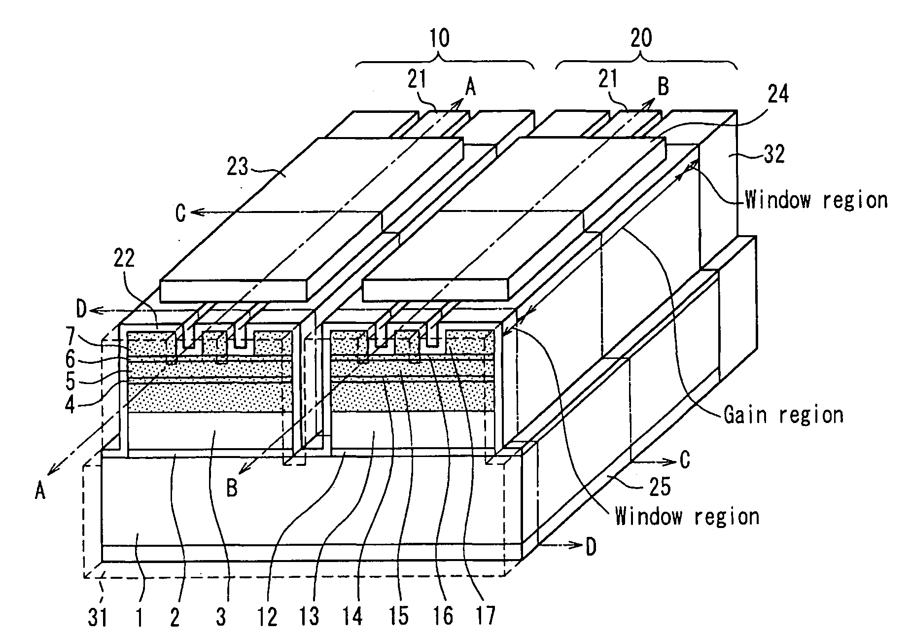
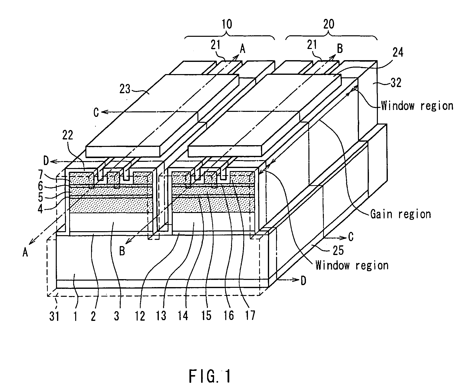
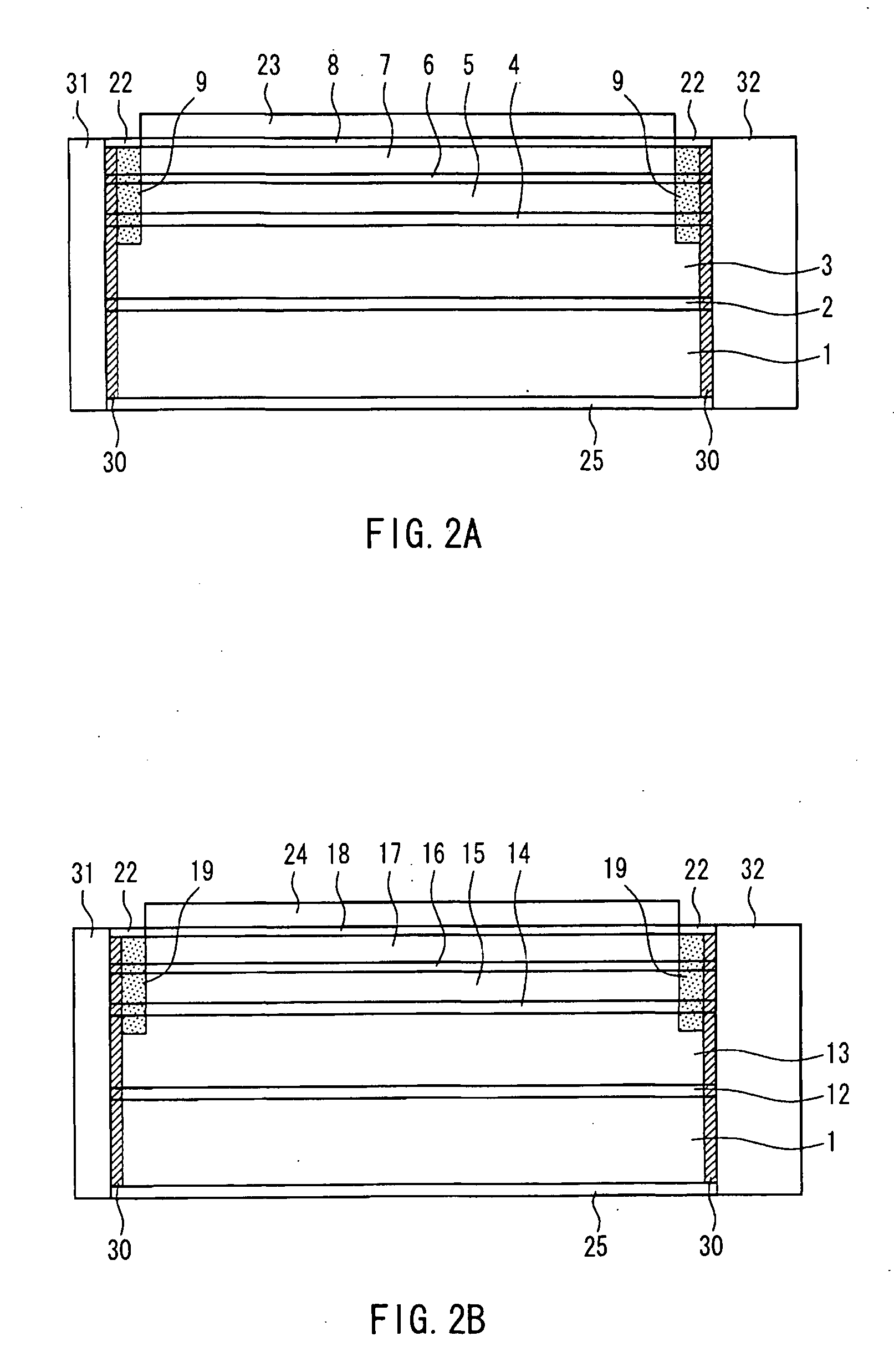
[0036]In the semiconductor laser device of the present invention, it is preferable that a facet window structure in which the first quantum well structure or the second quantum well structure is disordered is formed on at least one of the facets of the first resonator and the second resonator.

[0037]Moreover, it is possible to adopt a configuration in which the disordering is formed with impurity of Zn or Si.

[0038]Moreover, it is possible to adopt a configuration in which a constituent material of the first active layer is AlxGa1-xAs (0≦x≦1), and a constituent material of the second active layer is (AlxGa1-x)yIn1-yP (0≦x≦1, 0≦y≦1).

[0039]Moreover, it is possible to adopt a configuration in which the first upper cladding layer and the second upper cladding layer are made of AlxGa1-xAs (0≦x≦1) or (AlxGa1-x)yIn1-yP (0≦x≦1, 0≦y≦1).

[0040]It is preferable to adopt a...


PUM


Abstract

On a first region that is a part of one main face of a semiconductor substrate 1, a first semiconductor laser structure 10 is formed so as to have a first lower cladding layer 3, a first active layer 4 with a first quantum well structure and first upper cladding layers 5, 7, which are layered in this order from the semiconductor substrate side, thereby forming a first resonator. On a second region that is different from the first region, a second semiconductor laser structure 20 is formed so as to have a second lower cladding layer 13, a second active layer 14 with a second quantum well structure and a second upper cladding layer 15, 17, which are layered in this order, thereby forming a second resonator. End face coating films 31, 32 are formed on facets of the first and the second resonators, and a nitrogen-containing layer 30 is formed between the facets of the first and the second resonators and the facet coating film. In the semiconductor laser device provided with a high-output dual-wavelength lasers that are formed monolithically, the decrease of the COD level during the high-output operation of the laser can be suppressed.

Description

BACKGROUND OF THE INVENTION[0001]1. Field of the Invention[0002]The present invention relates to a semiconductor laser device, and particularly relates to a monolithic type semiconductor device that has a plurality of emitting points, and a method for manufacturing the same.[0003]2. Description of Related Art[0004]As pick-up light sources for optical disk devices and light sources for optical information processing, optical communication and optical measurement, semiconductor laser devices are used. For example, as a pick-up light source for reproducing and recording with respect to a CD (compact disk) and a MD (mini disk), an infrared laser with a wavelength in the 780 nm band is used, and as a pick-up light source for reproducing and recording with respect to a DVD (digital video disk) with a higher density, an infrared laser with a wavelength in the 650 nm band is used.[0005]In order to be compatible with a CD, a MD and a DVD, both an infrared laser and a red laser are necessary ...

Claims


Application Information

Patent Timeline
Patent Type & Authority Applications(United States)
IPC IPC(8): H01S5/026H01S5/20H01L21/02
CPCB82Y20/00H01S5/028H01S5/0281H01S5/162H01S5/4087H01S5/34313H01S5/34326H01S5/4031H01S5/32316
Inventor YOKOYAMA, TAKESHIKASHIMA, TAKAYUKIMAKITA, KOUJI
Owner PANNOVA SEMIC
Why Eureka
Try Eureka