Process for fabricating a field-effect transistor with doping segregation used in source and/or drain

a field-effect transistor and doping segregation technology, applied in the direction of semiconductor devices, electrical apparatus, semiconductor/solid-state device details, etc., can solve the problem of plow approach, achieve low work function, improve transistor performance, and improve the effect of transistor performan

Inactive Publication Date: 2009-04-23
ACORN TECH INC
View PDF4 Cites 11 Cited by
  • Summary
  • Abstract
  • Description
  • Claims
  • Application Information

AI Technical Summary

Benefits of technology

[0020]While the material that replaces the silicide may be silicon or another semiconductor material, of particular interest is the replacement with either a metal or a metal in conjunction with a separation layer in accordance with the methods and systems described in U.S. Pat. Nos. 6,833,556 and 7,084,423, each assigned to the assignee of the present invention. The resulting electrical device may be referred to as an AXFET. The separation layer material enhances device performance, in part by passivating the silicon surface after the removal of the silicide, and by reducing the effect of the Schottky barrier and the Fermi level pinning between the deposited metal and the semiconductor of the body, both of which effects will improve transistor performance compared with a metal / source drain device without the separation layer.
[0021]Metal source / drain devices suffer from reduced current due to the Schottky barrier at the metal / semiconductor interface. Doping proximate to a metal / semiconductor contact, for example between a S / D of a FET and its channel, increases the current through that contact, by increasing the degree of tunneling through the potential barrier (“Schottky barrier”) which forms in the semiconductor. Dopant adjacent to the separation layer of an AXFET may also improve the performance of devices using this technology.
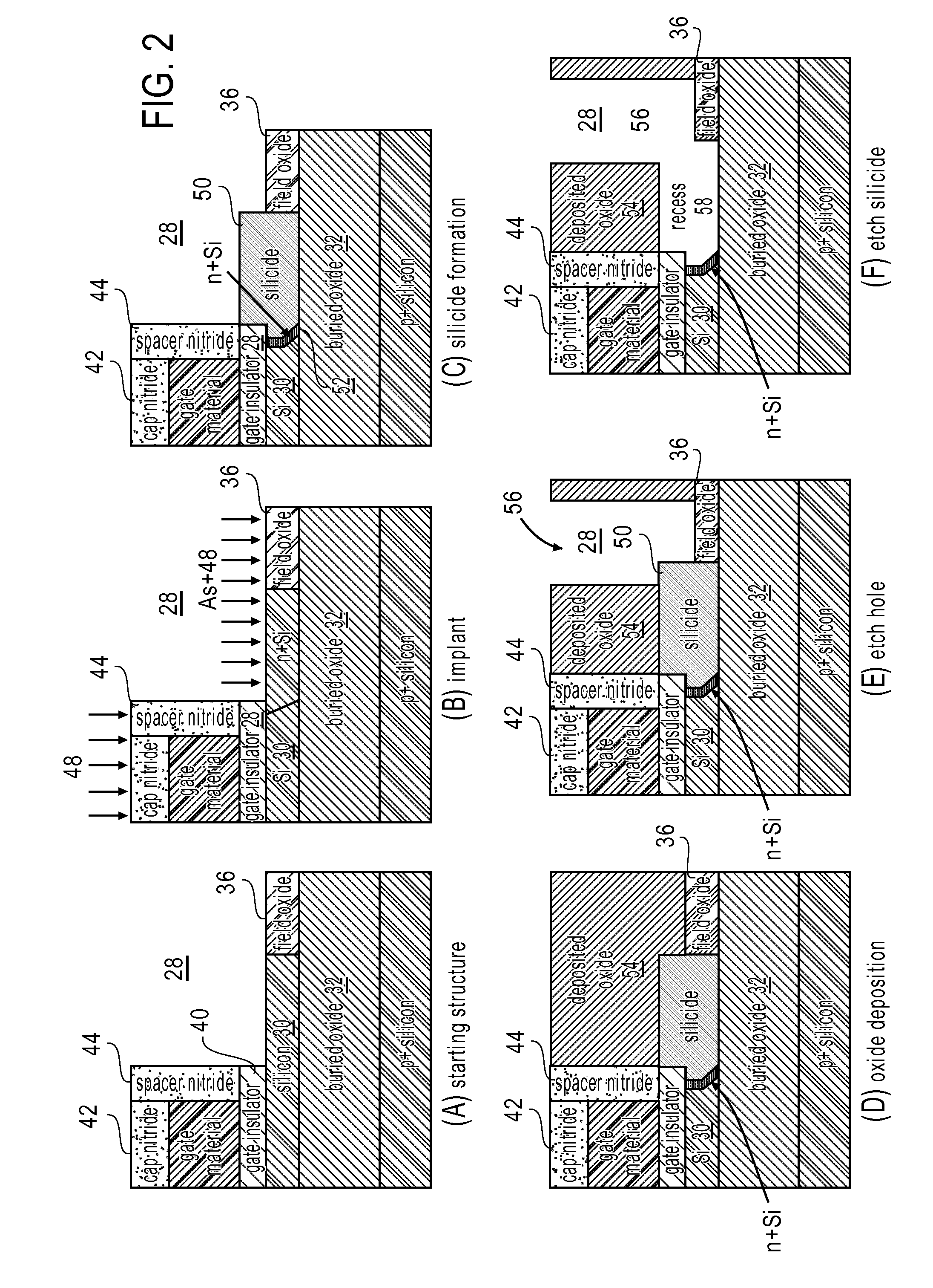
[0022]By using a chemical reaction to form a localized, relatively high concentration of dopant ions, then replacing the reaction product with one or more other materials, typically including at least one metal, a deposited S / D FET can be fabricated with reduced net “on-state” resistance compared with the resistance without the doping. Using this approach (instead of a more conventional approach such as ion implantation) affords the possibility of realizing many of the advantages of metal S / D or AXFET devices in both bulk silicon and ultra-thin-body FETs, while overcoming the limitations of a Schottky barrier between the metal and the semiconductor channel. It is preferable that the dopant layer should be formed by a process of segregation rather than diffusion such that the dopant layer has a very narrow profile rather than the less abruptly declining distribution typical of a
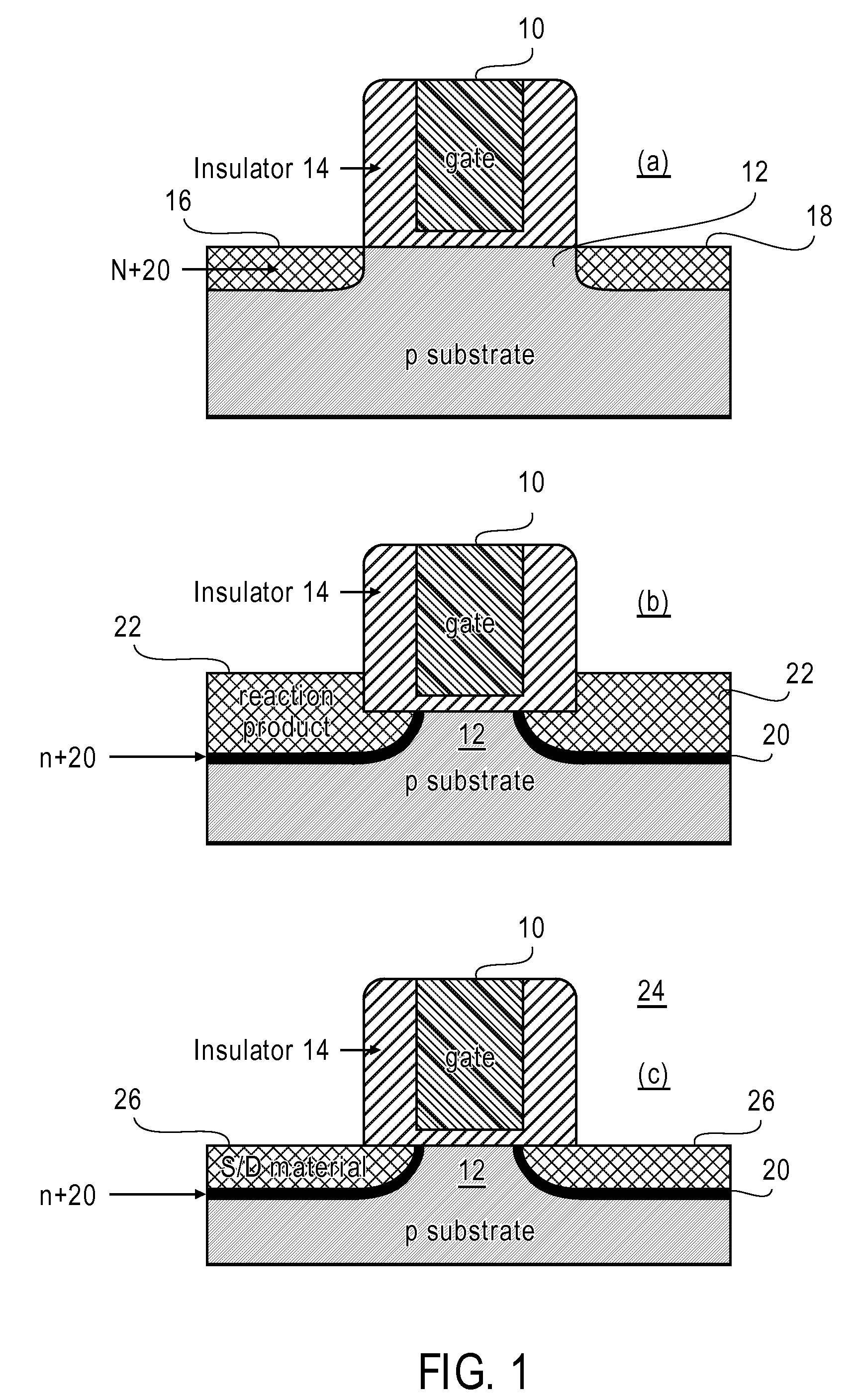
 diffusion profile.
[0023]It may be advantageous to construct integrated circuits consisting of both n-channel and p-channel devices, but using the above method for only one type of device. A specific example is the use of arsenic for the n-type dopant and boron for the p-type dopant. The source and drain regions are first doped, and then platinum silicide is formed. Platinum silicide will snow-plow both the arsenic and the boron to the desired region in the body of both the n-type and p-type transistors. Platinum silicide has a high work function, which is desirable for p-type devices but not for n-type devices. Next, the platinum silicide is removed from the source and drain regions of the transistors that are intended to be n-type devices, while leaving the platinum silicide in the source and drain regions of the p-type devices. After the removal, a metal or a metal and a separation layer (i.e., an AXFET structure) are deposited. Published data suggest that the p-type devices with a thin boron layer adjacent to the platinum silicide will have good performance. This method, therefore, produces integrated circuits with good performance for both n- and p-type transistors.
[0025]A further embodiment of the present invention provides for forming a FET as above, in which the reaction product is replaced, in whole or in part, with one or more metals, and a separation layer between the metal(s) and the doped semiconductor that remains after the reaction product is removed. The separation layer may serve to passivate the semiconductor surface that remains after the reaction product is removed, and may also beneficially separate the metal(s) from the semiconductor surface to improve the transistor's performance.
[0027]A further embodiment of the present invention provides a FET that includes a semiconductor body and one or more metals in the source and drain regions, with the metal immediately adjacent to the semiconductor body having a low work function for n-type transistors and a high work function for p-type transistors, and including both a thin separation layer between the metal(s) and the body, and also a thin layer of dopant in the body immediately adjacent to the separation layer. The separation layer may improve performance compared with devices constructed in the same manner but without such a separation layer. The thin dopant layer may also improve performance compared with similarly constructed devices that do not have this dopant layer, with or without the separation layer.

Problems solved by technology

One limitation of the snow-plow approach, as demonstrated to date, is that it requires the selection of a single silicide for both n-FETs and p-FETs.

Method used


Image

  • Process for fabricating a field-effect transistor with doping segregation used in source and/or drain
  • Process for fabricating a field-effect transistor with doping segregation used in source and/or drain
  • Process for fabricating a field-effect transistor with doping segregation used in source and/or drain

Examples


Embodiment Construction

[0035]Discussed herein is a method for forming a FET using impurity segregation in one or more sources and / or drains, and replacing the reacted material with one or more other materials.

[0036]In one embodiment of the invention, one or more of the source(s) and / or drain(s) of the FET is formed so that impurities, for example donor impurities for an n-type source and / or drain, or for example acceptor impurities for a p-type source and / or drain, are incorporated into the semiconductor in the region in which one or more source(s) and / or drain(s) is to be formed. For example, ion implantation can be used to cause the impurities to be placed in exposed semiconductor, using a self-aligned process. Or, for example, a layer rich in the desired impurity or impurities may be placed proximate to the semiconductor in the region in which the source(s) and / or drain(s) is to be formed, then heat may be applied to cause the impurity or impurities to diffuse into the proximate semiconductor. Or, for ...


PUM


Abstract

Source and / or drain regions of a transistor are first doped with an appropriate dopant and a metal is subsequently deposited. After heating, a silicide will displace the dopant, creating an increased density of dopants at the border of the silicided region. The dopants that are adjacent to or in the gate region of the device will form a thin layer. The silicide or other reactant material is then removed and replaced with a desired source / drain material, while leaving the layer of dopant immediately adjacent to the newly deposited source / drain material.

Description

RELATED APPLICATIONS[0001]This is a NON-PROVISIONAL of and claims priority to U.S. Provisional Patent Application No. 60 / 980,719, filed 17 Oct. 2007, incorporated herein by reference.FIELD OF THE INVENTION[0002]The present invention relates to processes for forming insulated-gate field-effect transistors using impurity segregation in one or more sources and / or drains, and replacing the reacted material with one or more other materials.BACKGROUND[0003]An insulated gate field-effect transistor (“IGFET”) is a semiconductor-based device in which the charge in one or more channels in one or more semiconductors is controlled by the charge and / or potential at one or more gates, and where the one or more channels are each proximate to one or more source(s) and / or drain(s), wherein a source or drain (“S / D”) is a conducting region providing electrical contact to one or more proximate channels. A semiconductor channel consists of the carriers which are present when the transistor is in one or ...

Claims


Application Information

Patent Timeline
Patent Type & Authority Applications(United States)
IPC IPC(8): H01L21/8238H01L23/62
CPCH01L21/26513H01L21/823814H01L21/84H01L27/1203H01L29/41791H01L29/665H01L29/66636H01L2924/0002H01L29/66795H01L29/785H01L29/78618H01L2029/7858H01L2924/00
Inventor GAINES, R. STOCKTONNISHI, YOSHIOCONNELLY, DANIEL J.CLIFTON, PAUL
Owner ACORN TECH INC
Why Eureka
Try Eureka