

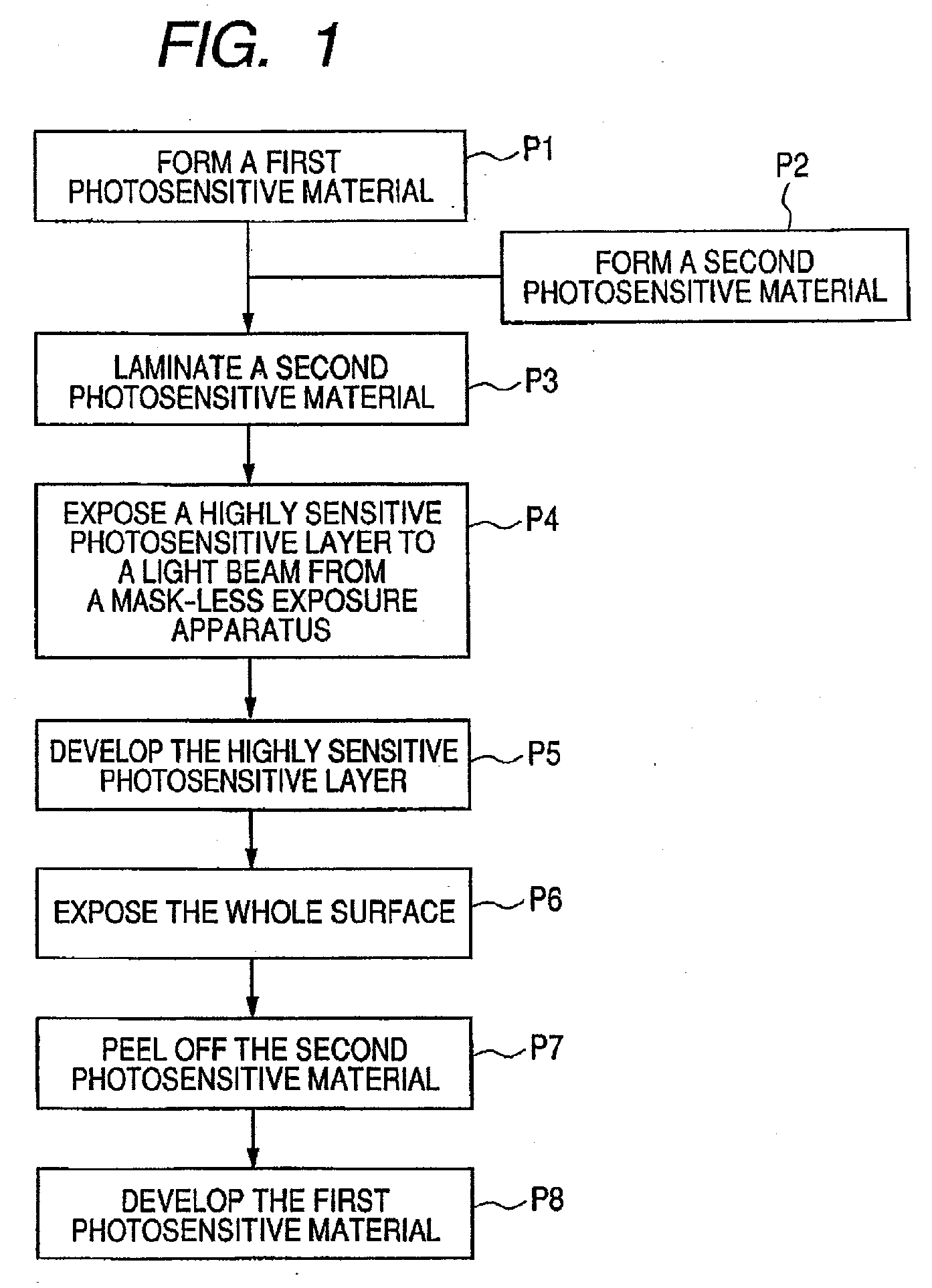
Pattern Formation Method
a pattern and pattern technology, applied in the field of photolithography methods, can solve the problems of increasing the cost and delay of product delivery, increasing the apparatus cost and running cost, and difficulty in drawing a high-precision pattern in a large area, so as to reduce the damage to the first photosensitive material 3
- Summary
- Abstract
- Description
- Claims
- Application Information
AI Technical Summary
Benefits of technology
Problems solved by technology
Method used
Image

Examples
examples
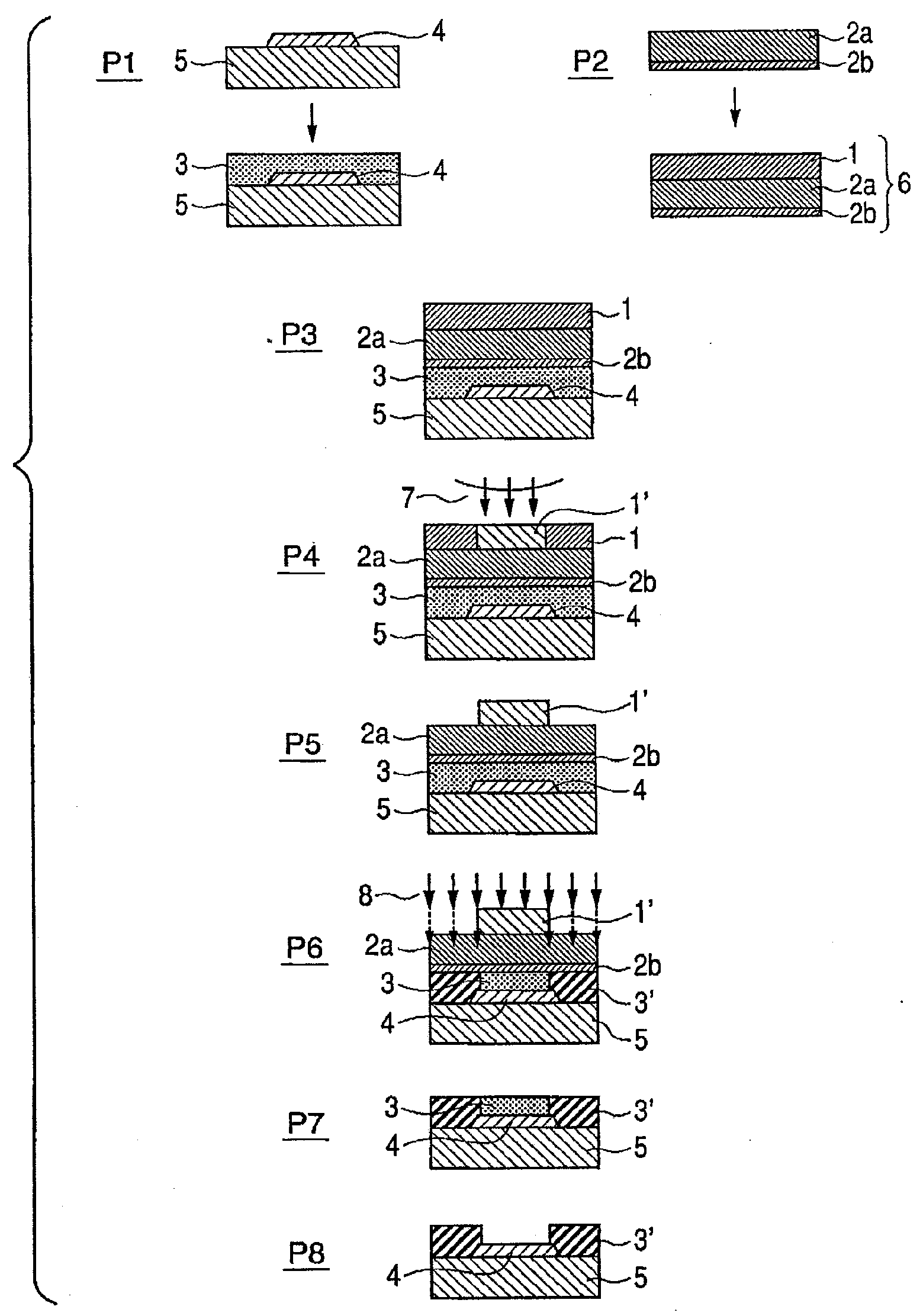
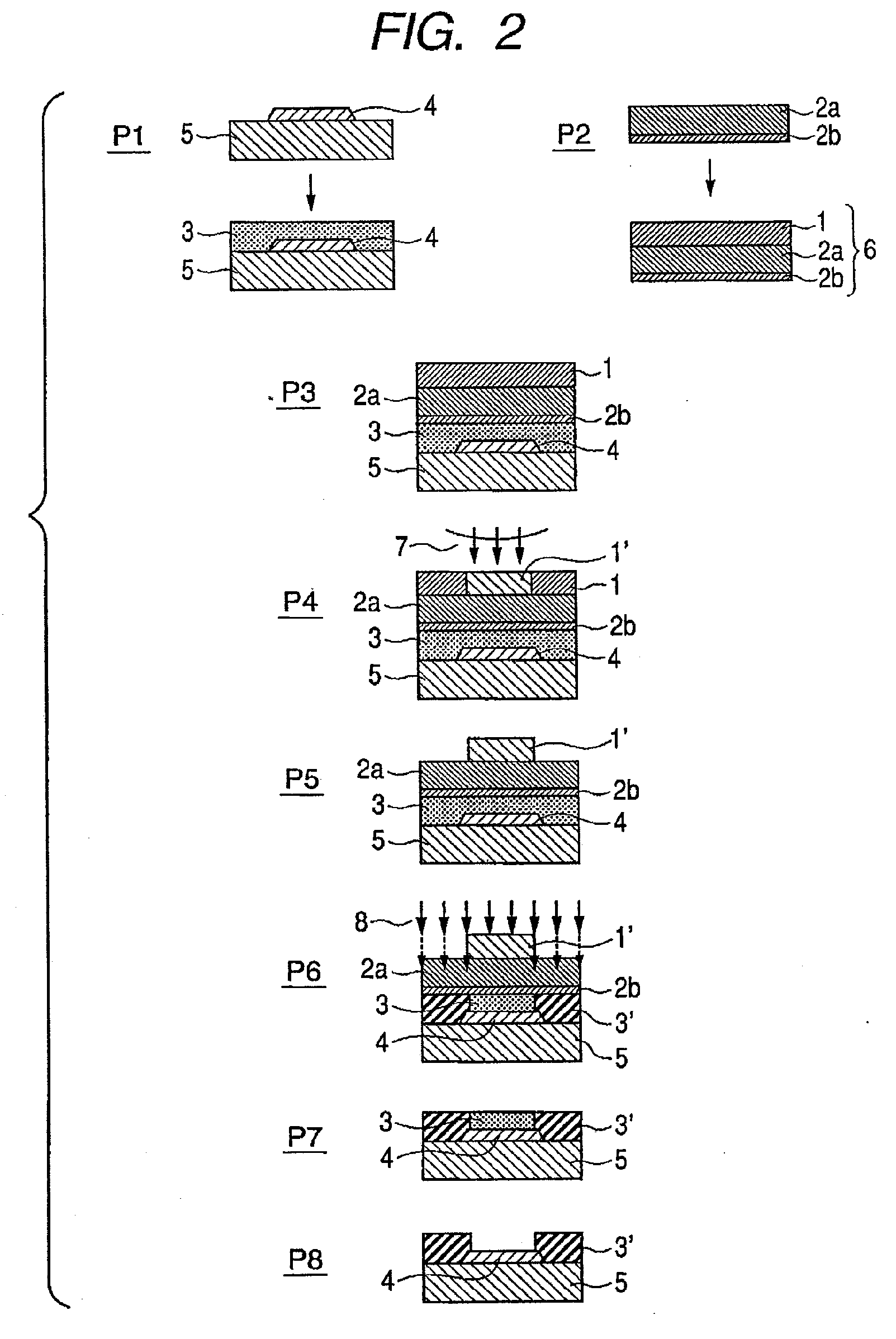
[0057]Examples of the pattern formation method according to the present invention are described below. An alkali-soluble negative type liquid photosensitive solder resist (produced by Hitachi Chemical Co., Ltd.: SR7200G) as a first photosensitive material 3 was applied, with a film thickness of about 25 μm, to a laminate sheet 5 with the both surfaces plated with copper and having a thickness of 0.5 mm to form an object for exposure to a light beam.
[0058]A highly sensitive photosensitive layer 1 is prepared by having silver bromide particles contained therein, with the silver bromide particle including a silver iodide of 5 mol % such that a volume ratio between the silver bromide particle and a gelatin solution is 0.6. The thus-formed highly sensitive photosensitive layer 1 is coated onto a polyethylene telephthalate (PET) film 2a with a thickness of 100 μm such that silver is deposited by 0.3 mol / m2 to form a second photosensitive material 6. The second photosensitive material 6 wa...
PUM
| Property | Measurement | Unit |
|---|---|---|
| temperature | aaaaa | aaaaa |
| wavelength range | aaaaa | aaaaa |
| wavelength | aaaaa | aaaaa |
Abstract
Description
Claims
Application Information