
High-mobility trench mosfets

Active Publication Date: 2009-05-07
ALPHA & OMEGA SEMICON LTD
View PDF12 Cites 33 Cited by
  • Summary
  • Abstract
  • Description
  • Claims
  • Application Information

AI Technical Summary

Benefits of technology

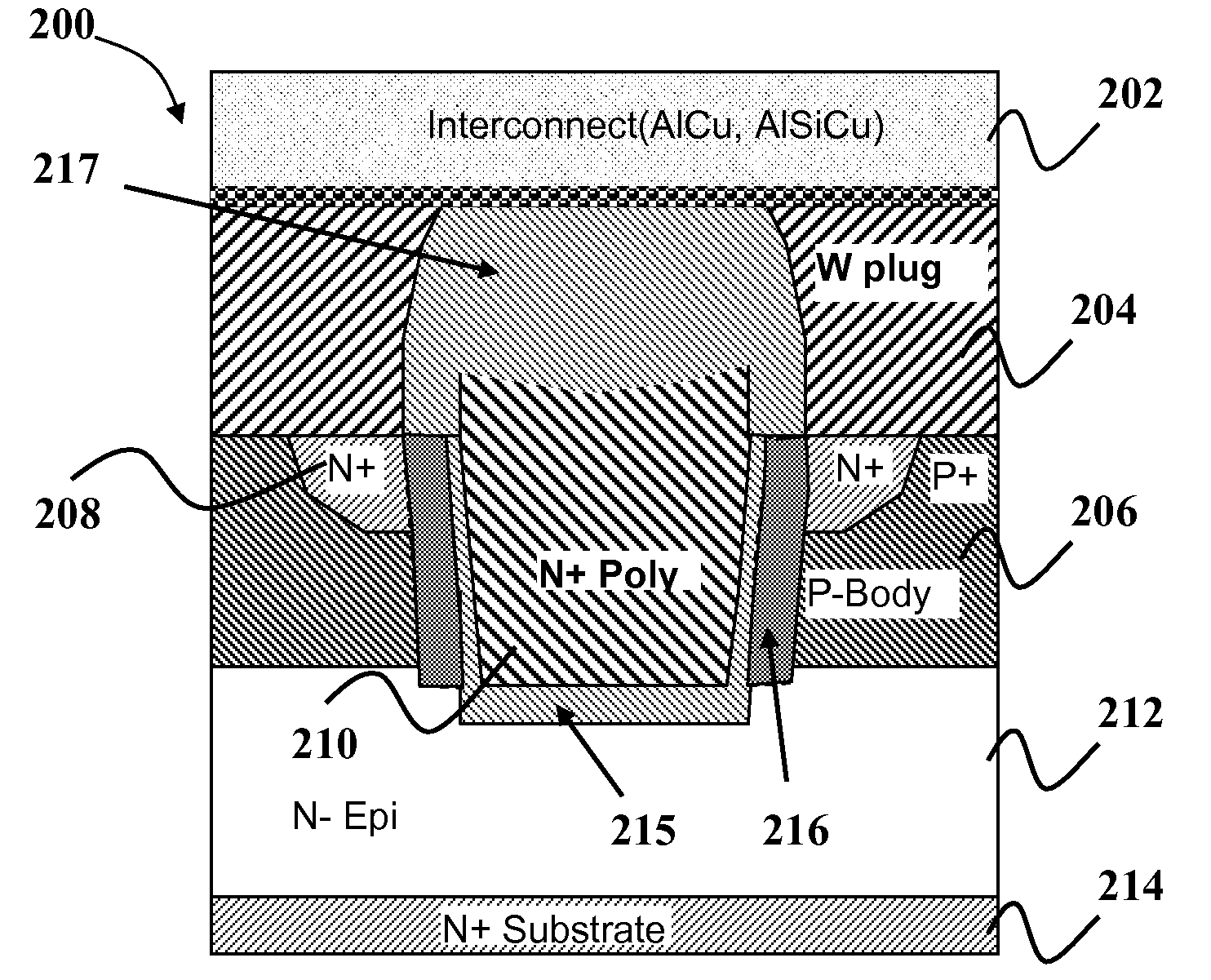
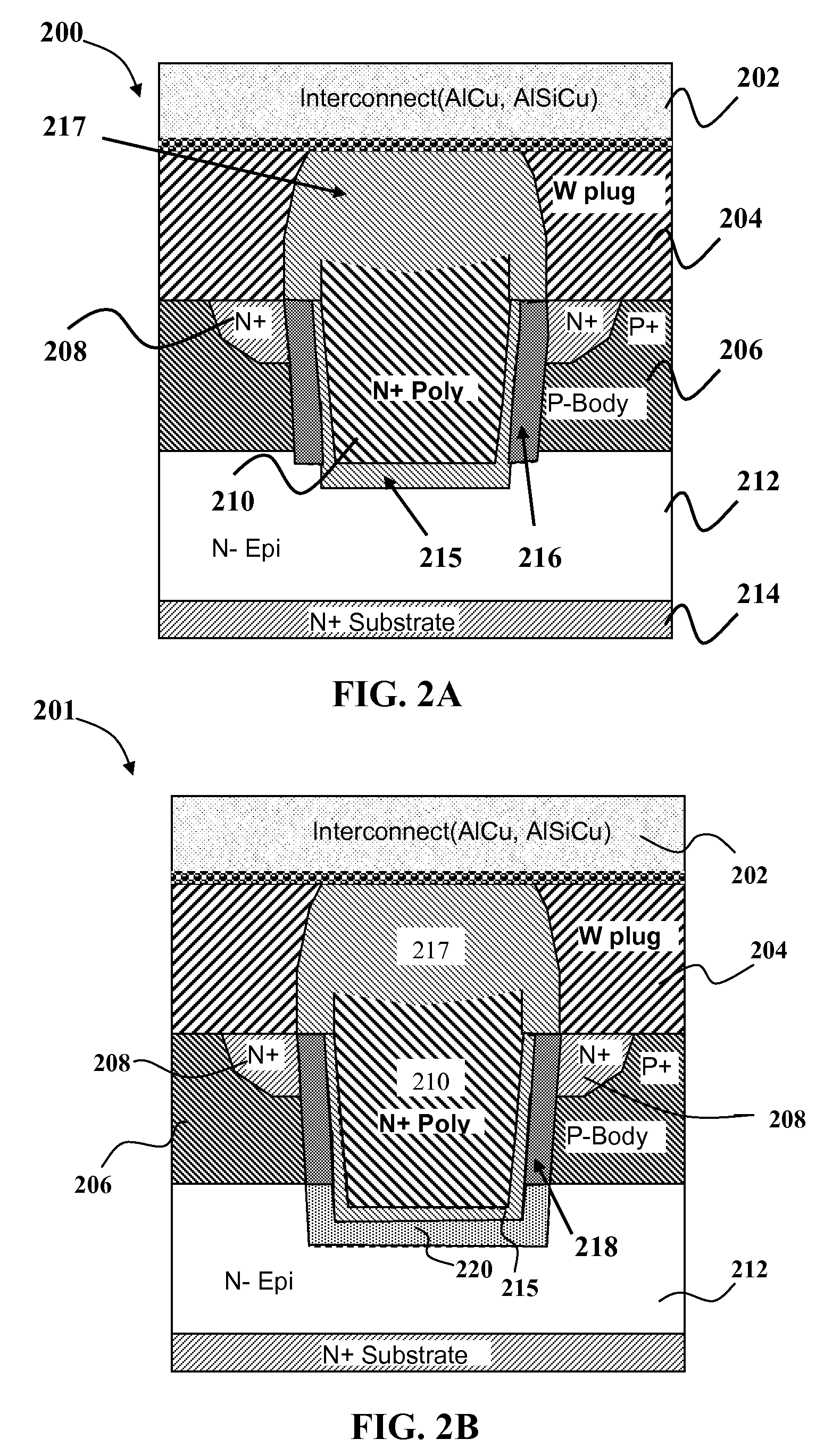
[0021]According to embodiments of the present invention, high mobility trench-DMOS field effect transistors, with single gate or shielded gate structure, may be achieved through use of a SiGe sidewall channel and / or a channel strained by SiGe-Source or SiGe-Source-Drain regions applied to NMOS and PMOS vertical channel trench structures. SiGe has recently become widely available in multiple Silicon Semiconductor Facilities. The advantages of using SiGe in low voltage (LV) trench-DMOSFETS include high-mobility the in channel region and minimizing Rdson, small cell pitch by using vertical channel structures, high-power density when combined with Vertical MOSFET technology (drain at bottom).
[0024]FIG. 2C is a cross-sectional view of a gate trench DMOSFET 203 according to an alternative embodiment of the present invention. The gate trench DMOSFET 203 uses a SiGe-source to produce a strained channel strained channel. The structure of the DMOSFET 203 is similar to that shown in FIG. 2A. In the DMOSFET 203, however, SiGe source regions 219 may be configured to induce a unidirectional uniaxial compressive strain structure within a silicon channel. Similar to the DMOSFET 200 of FIG. 2A, the DMOSFET 203 includes an N+ substrate 214, upon which is grown a lightly doped n-epitaxial layer 212 of a predetermined thickness functioning as drain region. Within the N-epi layer 212, P-body region 206 (p, p+) is provided. The DMOSFET 203 also includes a N+ poly trench gate 210 insulated from the P-body layer 206 and source regions 208 by a gate oxide layer 215 and insulated from metal plug layer 204 by an oxide layer 217. A conductive layer 202 e.g., made of AlCu or AlSiCu, overlying most of the W plug layer 204 serves as source. N+ type strained SiGe source regions 219 are provided on top of the P-body region 206. A lattice mismatch between the N+ SiGe and the P+ silicon material of the body layer 206 on the sides induces strain in a channel region 222 proximate the trench sidewalls. The strain in the channel region 222 increases mobility for charge carriers in the channel region.
[0050]As shown in FIG. 8B, a trench 809 may be formed by reactive ion etching (RIE) through one or more openings in the hardmask 808. The trench 809 preferably penetrates through the P-body layer 806 such that the bottom of the trench 809 reaches the N-epi layer 804. As shown in FIG. 8C, undoped SiGe layer 810, may be formed, e.g., using blanket deposition or selective growth, e.g., of polycrystalline-SiGe on oxide layer 808 and single crystalline-SiGe on exposed silicon of P-body layer 806 on the sides of the trenches 809, and N-epi layer 804 at the bottom of the trench 809. The SiGe growth can be performed after an optional sacrificial oxide growth and etch, to improve the crystalline quality at the surface of the trenches. An oxide layer 812 may then be deposited on the top of the undoped SiGe layer 810 as shown in FIG. 8D.

Problems solved by technology

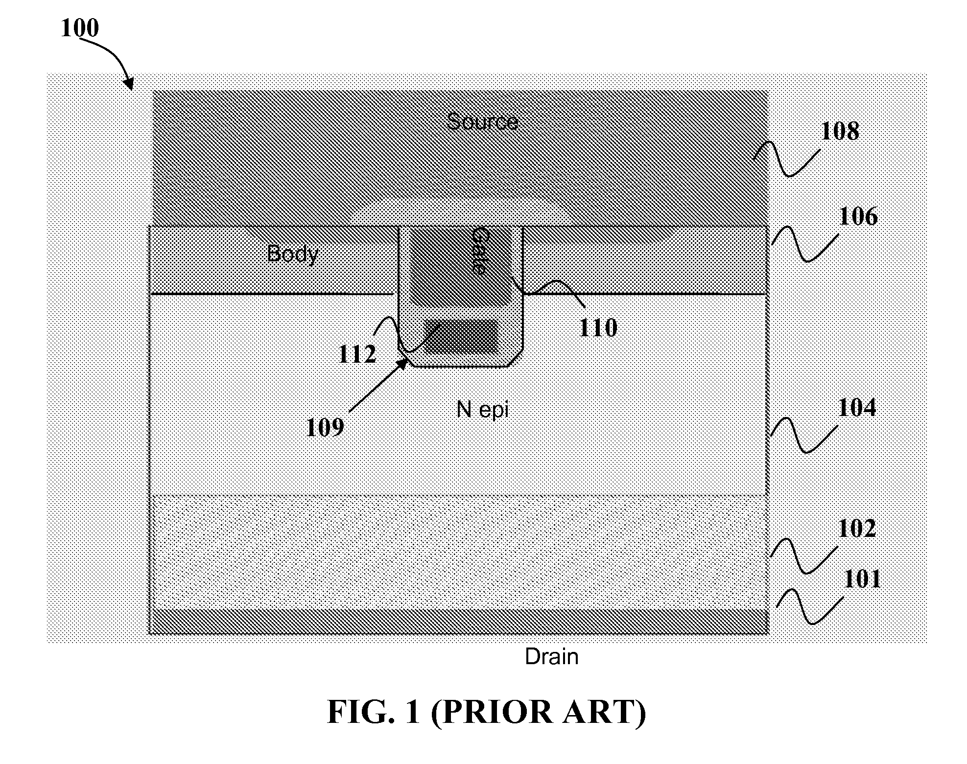
A problem with prior art trench DMOS transistors is that the channel mobility tends to remain low (especially P channel devices) due to the limited mobility of silicon.
There is no improvement in mobility for standard MOSFETs; therefore, drain to source resistance Rdson can be significant at low voltages.
Unfortunately, in addition to relatively low channel mobility, planar MOSFETs tend to have a large cell pitch because of the horizontal structure of the channel and drain, source and gate.

Method used


Image

  • High-mobility trench mosfets
  • High-mobility trench mosfets
  • High-mobility trench mosfets

Examples


Embodiment Construction

[0020]Although the following detailed description contains many specific details for the purposes of illustration, anyone of ordinary skill in the art will appreciate that many variations and alterations to the following details are within the scope of the invention. Accordingly, the exemplary embodiments of the invention described below are set forth without any loss of generality to, and without imposing limitations upon, the claimed invention.

[0021]According to embodiments of the present invention, high mobility trench-DMOS field effect transistors, with single gate or shielded gate structure, may be achieved through use of a SiGe sidewall channel and / or a channel strained by SiGe-Source or SiGe-Source-Drain regions applied to NMOS and PMOS vertical channel trench structures. SiGe has recently become widely available in multiple Silicon Semiconductor Facilities. The advantages of using SiGe in low voltage (LV) trench-DMOSFETS include high-mobility the in channel region and minimi...


PUM


Abstract

High-mobility vertical trench DMOSFETs and methods for manufacturing are disclosed. A source region, a drain region or a channel region of a high-mobility vertical trench DMOSFET may comprise silicon germanium (SiGe) that increases the mobility of the charge carriers in the channel region. In some embodiments the channel region may be strained to increase channel charge carriers mobility.

Description

FIELD OF THE INVENTION[0001]This invention generally relates to trench-metal oxide silicon field effect transistors (trench-MOSFETs) and more particularly to high-mobility trench-MOSFETs.BACKGROUND OF THE INVENTION[0002]A DMOS (Double Diffused MOS) transistor is a type of MOSFET (Metal Oxide Semiconductor Field Effect Transistor) that uses diffusion to form the transistor region. DMOS transistors are typically employed as power transistors for power integrated circuits. DMOS transistors provide high current per unit area where low forward voltage drops are required.[0003]One particular type of DMOS transistor is a so-called “trench” DMOS transistor in which the channel is formed vertically and the gate is formed in a trench extending between the source and drain. The trench, which is lined with a thin oxide layer and filled with polysilicon (i.e., polycrystalline silicon), allows less constricted current flow and thereby provides lower values of specific on-resistance. Examples of t...

Claims


Application Information

Patent Timeline
IPC IPC(8): H01L29/778H01L21/336
CPCH01L29/1054H01L29/165H01L29/4236H01L29/7813H01L29/456H01L29/66734H01L29/42368H01L29/7848
Inventor HEBERT, FRANCOIS
Owner ALPHA & OMEGA SEMICON LTD
Learn More