Light emitting devices with phosphor wavelength conversion and methods of fabrication thereof
a technology of light emitting devices and phosphor wavelength, which is applied in the direction of semiconductor devices, semiconductor/solid-state device testing/measurement, coatings, etc., can solve the problems of increased production costs, supply chain challenges for white led suppliers and customers, and the human eye is extremely sensitive to subtle changes. , to achieve the effect of simplifying the method
- Summary
- Abstract
- Description
- Claims
- Application Information
AI Technical Summary
Benefits of technology
Problems solved by technology
Method used
Image
Examples
first embodiment
[0068]A method in accordance with the invention will be described in relation to the fabrication of a white light emitting device of a specific color temperature and hue. In the this patent specification color is defined in terms of chromaticity values such that a specific color is defined as having specific CIE xy chromaticity coordinates. It will be appreciated however, that other systems of defining color can be used with the method of the invention.
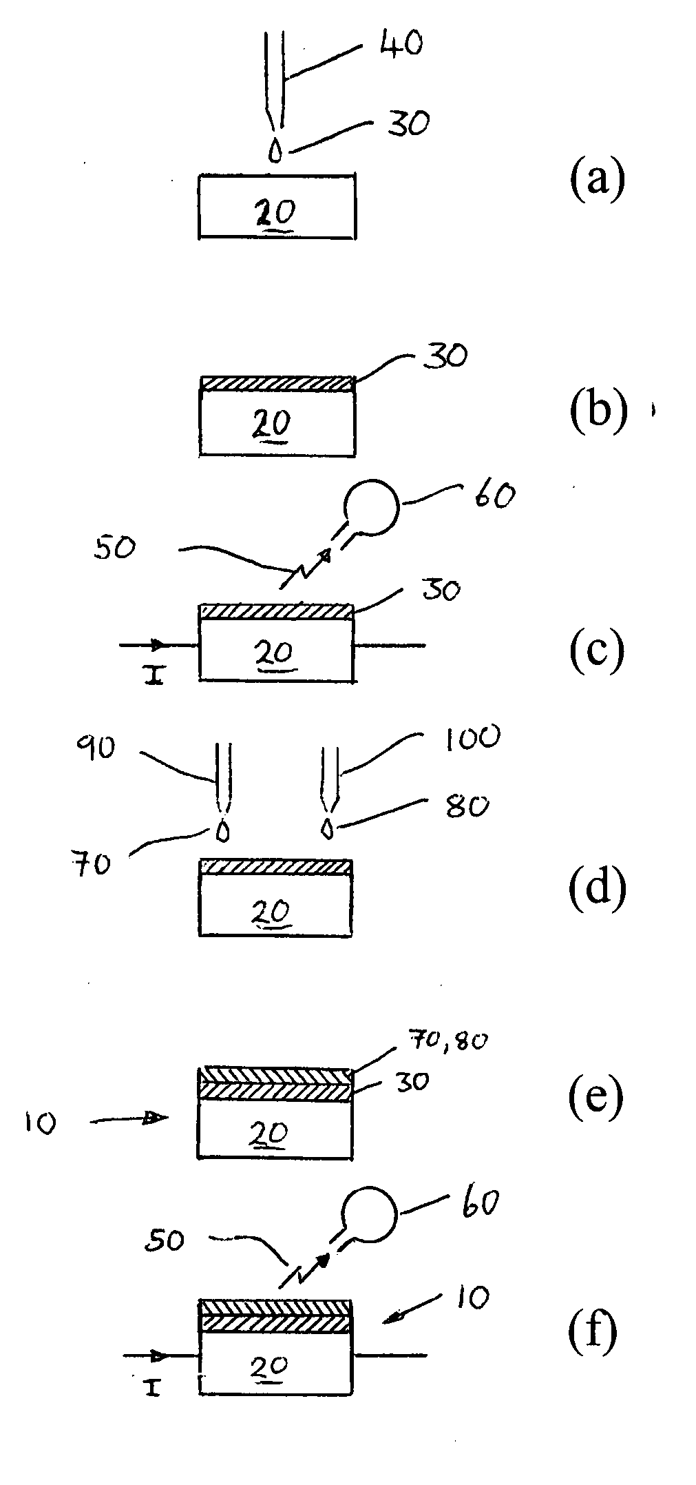
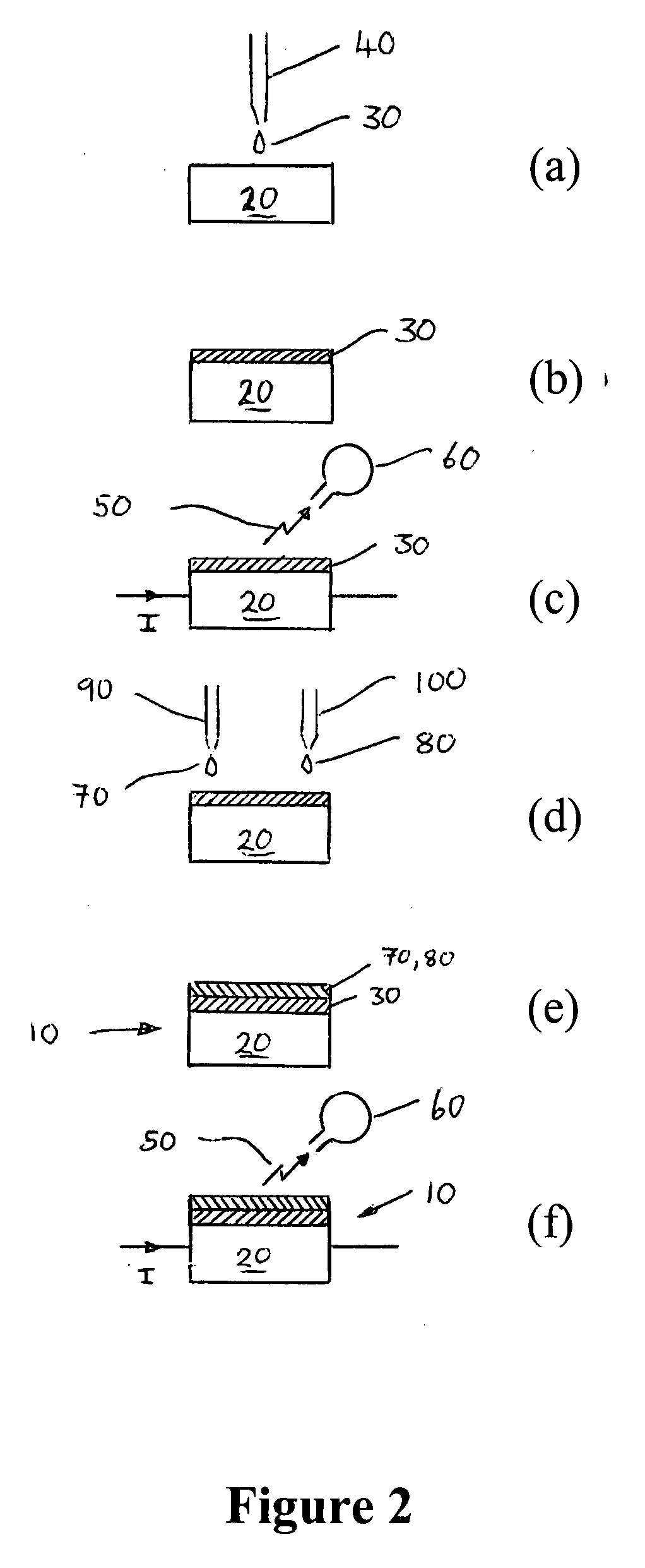
[0069]The white light device 10 comprises an LED chip 20 such as an InGaN / GaN (indium gallium nitride / gallium nitride) based LED chip that generates excitation radiation (light) of a first wavelength range, typically blue light of wavelength 400 to 465 nm. The device 10 further includes two different light emitting phosphor (photo-luminescent or wavelength conversion) materials that respectively convert at least a part of the light emitted by the chip into light of different colors such as for example yellow and green light. The blue ...
second embodiment
[0087]As with the first method, the method in accordance with the second embodiment can be used in the high volume production of light emitting devices and in the production of devices which comprise a plurality of LED chips. In the case of the latter, phosphor material can be selectively removed from one or more of the LED chips and the device can be optimized for net emitted light or each LED's light output color optimized.
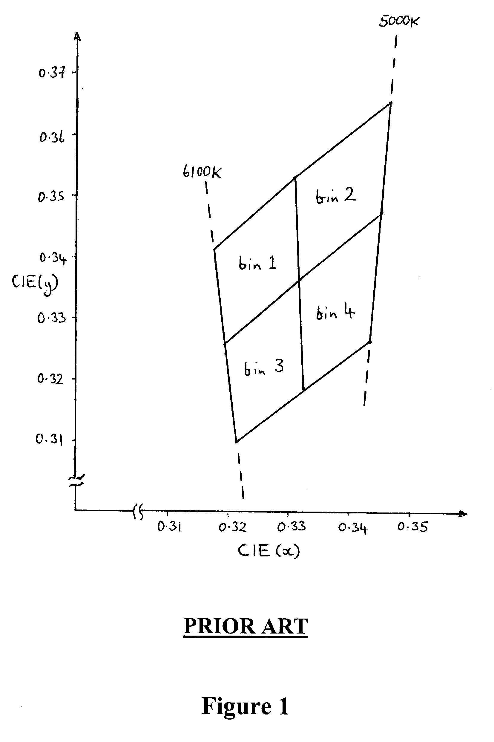
[0088]A particular benefit of the methods of the invention is that they can eliminate the need for binning. The methods of the invention are intended for use with inorganic phosphor materials such as for example silicate-based phosphor of a general composition A3Si(OD)5 or A2Si(OD)4 in which Si is silicon, O is oxygen, A comprises strontium (Sr), barium (Ba), magnesium (Mg) or calcium (Ca) and D comprises chlorine (Cl), fluorine (F), nitrogen (N) or sulfur (S). Examples of silicate-based phosphors are disclosed in our co-pending patent applications US2006 / 014512...
PUM
 Abstract
Description
Claims
Application Information


