Spin transfer MRAM device with separated CPP assisted writing

a technology of assisted writing and transfer mram, which is applied in the direction of semiconductor devices, digital storage, instruments, etc., can solve the problems of destroying a thin tunnel barrier layer such as mgo, difficult to apply a sufficient electric current to the address wiring, and a large electric current magnetic field in the device, so as to increase the read and write efficiency

Active Publication Date: 2009-05-21
TAIWAN SEMICON MFG CO LTD
View PDF13 Cites 54 Cited by
  • Summary
  • Abstract
  • Description
  • Claims
  • Application Information

AI Technical Summary

Benefits of technology

[0020]One objective of the present invention is to provide a Spin-RAM design which leads to an improved interaction between a free layer in a CPP cell that operates by a spin transfer effect and a free layer in an underlying MTJ cell to increase read and write efficiency compared with the prior art.
[0021]A second objective of the present invention is to provide a Spin-RAM circuit employing a plurality of Spin-RAM cells according to the first objective to achieve two Spin-RAM cells and two MTJ cells per bit cell and allow one MTJ cell to serve as a reference while reading the second MTJ, thereby avoiding an external reference cell.
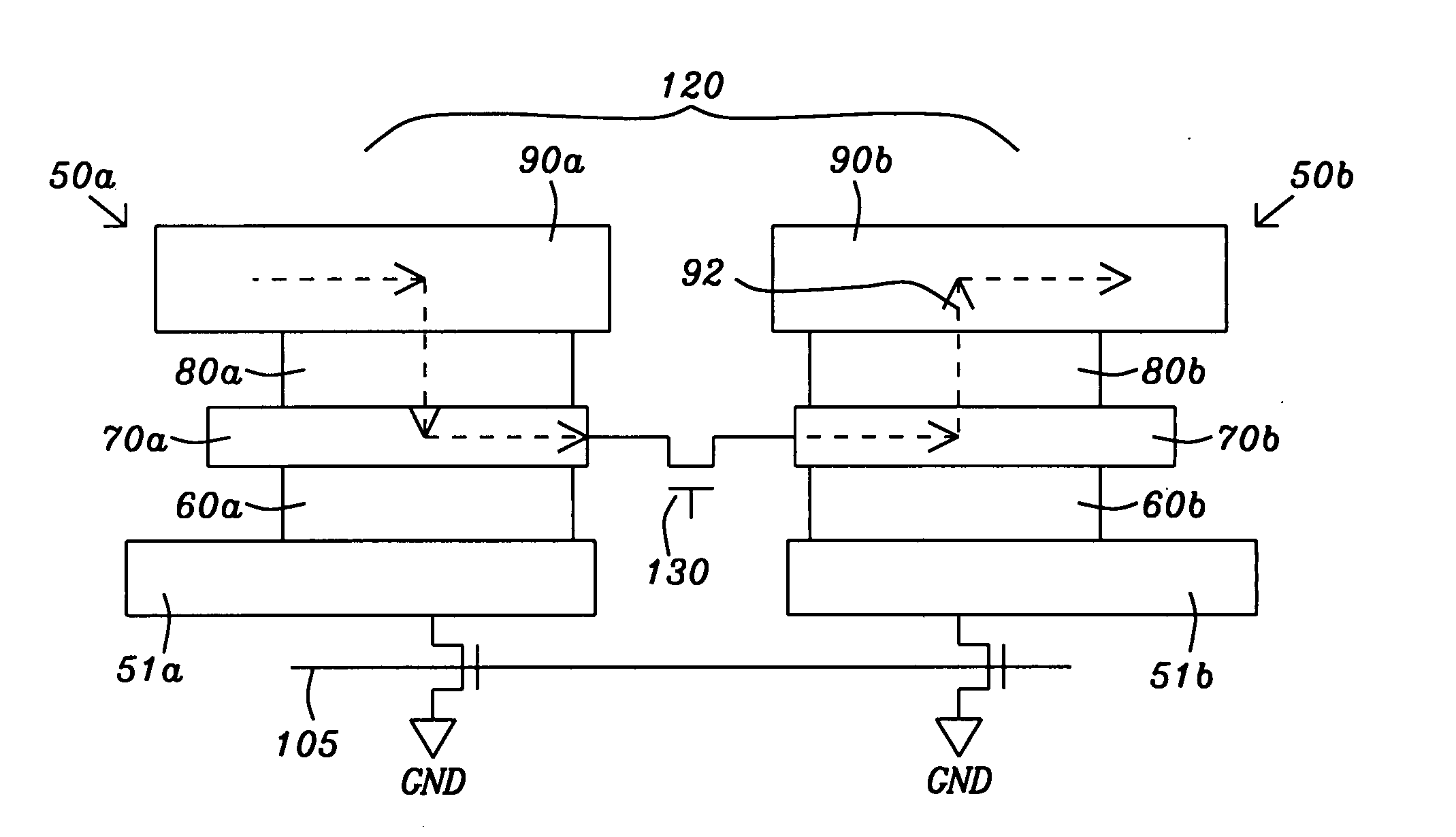
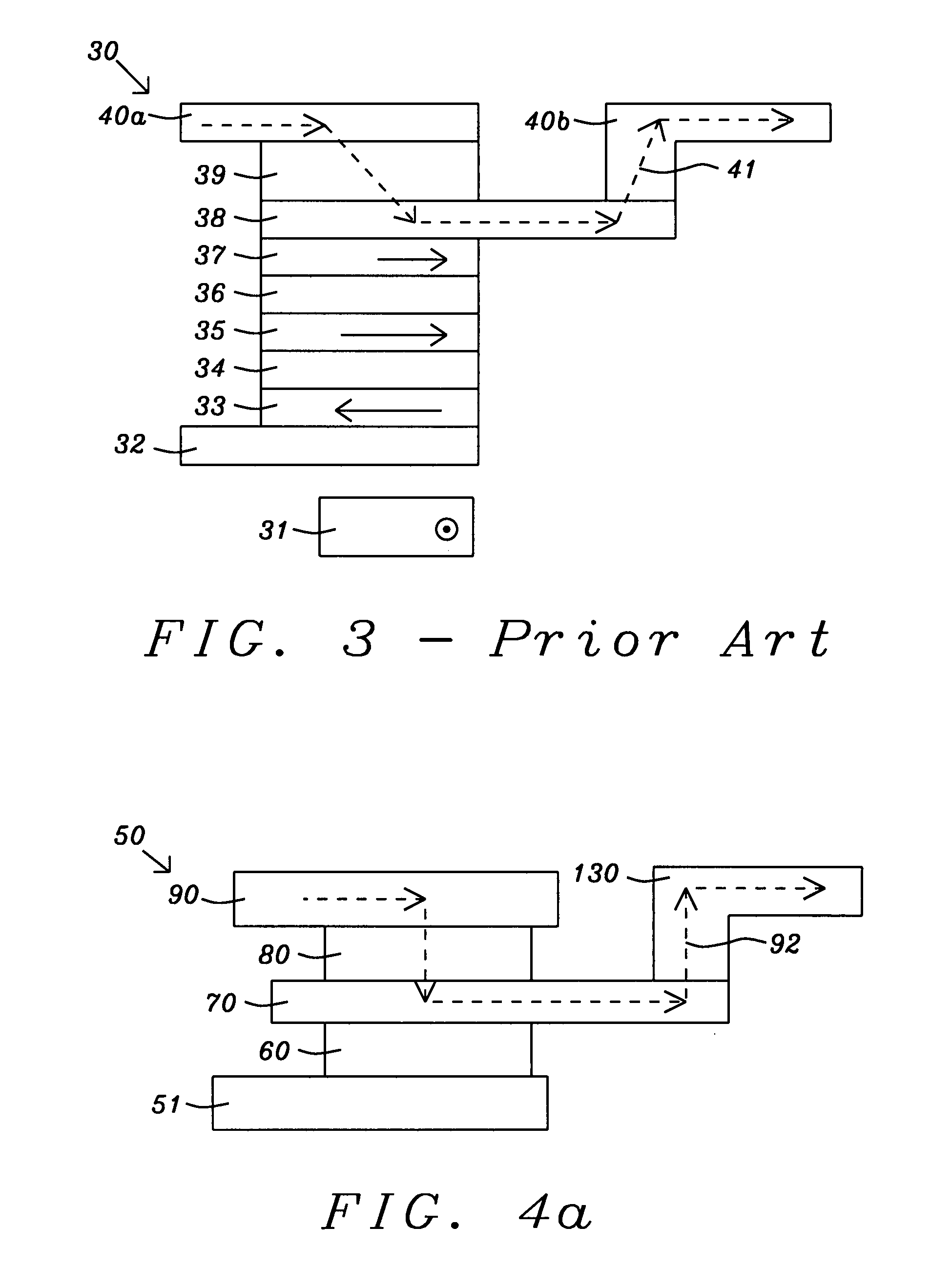
[0022]According to one embodiment, a more efficient Spin-RAM device is achieved with a bit cell configuration comprised of two CPP / MTJ sub-cells in which the two CPP / MTJ cells in each bit pair are written to opposite resistance states represented by (0,1) and (1,0). Each CPP / MTJ sub-cell has a stack comprised of a MTJ cell formed on a bottom electrode, a conductive spacer contacting the capping layer in the MTJ, a CPP cell formed on the conductive spacer, and a bit line contacting a capping layer in the CPP cell. Preferably, a first free layer in the MTJ cell has a small anisotropy of less than 5 Oe while a second free layer in the CPP cell has a large uniaxial anisotropy of at least 50 Oe or about 10× that of the first free layer. Thus, the large demagnetization field from the second free layer will easily switch the magnetic moment in the first free layer so that their magnetization directions are anti-parallel and will remain anti-parallel when the second free layer magnetization is switched during a write process. On the other hand, the first free layer will exert a relatively small field on the second free layer so as not to stabilize the CPP free layer. Consequently, the spin transfer switching of the second free layer by a write current can occur more easily than when the anisotropy of the first free layer and second free layer are closely matched. Furthermore, the anisotropy of the second free layer is large enough to assure a thermal factor KUMSV / kBT>40, where Ku is the anisotropy constant, Ms is the saturation magnetization, V is the second free layer volume, kB is the Boltzmann constant, and T is temperature.
[0023]The write current passes from a first bit line through a first CPP cell within the first CPP / MTJ sub-cell and into the conductive spacer which is connected through a transistor to a conductive spacer in a second CPP cell within a second CPP / MTJ sub-cell. In the second CPP cell, the write current passes from the conductive spacer through the second CPP cell to a second bit line that is grounded. The transistor is controlled by a write word line. When the magnetization in the second free layer in a CPP / MTJ sub-cell is switched by the write current, magnetic coupling will force the first free layer to switch magnetization as well and thereby remain anti-parallel to the magnetization in the second free layer. A high write current does not pass through the MTJ cell and avoids a tunnel barrier breakdown issue that has affected earlier Spin-RAM designs.
[0026]The present invention anticipates that the CPP cell and MTJ cell may be independently optimized so as to achieve a low write current in the CPP cell and a high dR / R in the MTJ. For instance, the CPP cell preferably has a larger size than the MTJ cell in order to take advantage of a large demagnetization field from the CPP free layer and thereby more efficiently switch the magnetic state in the MTJ free layer. Furthermore, the CPP cell may have a different shape than the MTJ cell. In one embodiment, the CPP cell has a large shape anisotropy derived from an elliptical or eye shape while the MTJ cell has an essentially round shape to promote a low anisotropy. A MTJ stack of layers may be laid down and patterned to form a MTJ cell followed by formation of a first dielectric layer adjacent to the MTJ cell. Subsequently, a second dielectric layer may be formed on the first dielectric layer and then the conductive spacer and write word line may be formed in the second dielectric layer. Thereafter, the CPP stack is deposited and patterned to form a CPP cell on the conductive spacer. Next, a third dielectric layer is deposited and made coplanar with the CPP cell. The bit line is then formed on the CPP cell by a conventional method.

Problems solved by technology

As memory devices are increasingly micro-miniaturized, the address wiring is also reduced in width so that it becomes difficult to apply a sufficient electric current to the address wiring.
Additionally, coercive force of the device is increased thereby leading to a greater electric current magnetic field and a higher power consumption in the device.
This high current density, which is required to induce the spin-transfer effect, could destroy a thin tunnel barrier layer such as AlOx, MgO, or the like.
Since write current also flows across the MTJ tunnel barrier layer, the reliability of MTJ cells becomes a large problem due to the fact that the MTJ will be damaged as the voltage across a MTJ junction reaches a threshold, the so-called breakdown voltage.
Additionally, a thin conducting spacer is very difficult to fabricate and a high current density flowing along the spacer layer would likely cause a reliability problem.
Also, as the MRAM dimension shrinks, it is becoming increasingly difficult during a read process to differentiate between a “0” and a “1” state when comparing the resistance in the MTJ cell to a reference cell in the periphery of the circuit.
However, this reference does not teach how the interaction between the two free layers can be optimized to improve switching efficiency.
Moreover, the memory device relies on a reference cell outside the bit cell during the read process which can slow the device speed.

Method used


Image

  • Spin transfer MRAM device with separated CPP assisted writing
  • Spin transfer MRAM device with separated CPP assisted writing
  • Spin transfer MRAM device with separated CPP assisted writing

Examples


Embodiment Construction

[0035]One aspect of the present invention is a CPP / MTJ sub-cell configuration within a Spin-RAM device that provides for a separation of write and read pathways so that the writing process and reading process can be independently optimized. In the CPP and MTJ cells, the exemplary embodiment depicts a single spin valve structure. However, the present invention also encompasses a CPP / MTJ sub-cell wherein one or both of the CPP cell and MTJ cell have a dual spin valve configuration. Devices based on this technology may be referred to as Spin-RAM or spin-transfer MRAM devices. Another aspect of the present invention is a wiring scheme comprised of a plurality of bit cells, word lines, and bit lines that takes advantage of a pair of CPP / MTJ sub-cells within each bit cell which enables the reading process to be more efficient. Those skilled in the art will appreciate that the terms “magnetic moment” and “magnetization direction” may be used interchangeably.

[0036]First, the CPP / MTJ sub-cel...


PUM


Abstract

A spin-transfer MRAM is described that has two sub-cells each having a conductive spacer between an upper CPP cell and a lower MTJ cell. The two conductive spacers in each bit cell are linked by a transistor which is controlled by a write word line. The two CPP cells in each bit cell have different resistance states and the MTJ cell and CPP cell in each sub-cell have different resistance states. The MTJ free layer rotates in response to switching in the CPP free layer because of a large demagnetization field exerted by the CPP free layer. An improved circuit design is disclosed that enables a faster and more reliable read process since the reference is a second MTJ within the same bit cell. When RMTJ1>RMTJ2, the bit cell has a “0” state, and when RMTJ1<RMTJ2, the bit cell has a “1” state.

Description

FIELD OF THE INVENTION[0001]The invention relates to a spin-transfer MRAM cell in which an upper CPP cell is separated from a lower MTJ cell by a conducting layer in order to form different read and write paths, and each bit cell has two spin-transfer MRAM cells that are written into opposite resistance states.BACKGROUND OF THE INVENTION[0002]Magnetoresistive Random Access Memory (MRAM), based on the integration of silicon CMOS with magnetic tunnel junction (MTJ) technology, is a strong candidate to provide a dense (8-25F2 cell size), fast (1˜30 ns read / write speed), and non-volatile storage solution for future memory applications. The MTJ utilizes a thin dielectric insulating layer like AlOx, AlNxOy, or MgOx that is formed between a first ferromagnetic layer which is pinned in a certain direction by an adjacent anti-ferromagnetic (AFM) layer, and a second ferromagnetic (free) layer. The pinned layer has a magnetic moment that is fixed in the “y” direction, for example, by exchange ...

Claims


Application Information

Patent Timeline
Patent Type & Authority Applications(United States)
IPC IPC(8): G11C11/00H01L21/00H01L29/82
CPCG11C11/16Y10S977/935H01L27/226G11C11/1659G11C11/161G11C11/1673G11C11/1675G11C11/1657H10B61/20
Inventor GUO, YIMINCHIEN, JEFF
Owner TAIWAN SEMICON MFG CO LTD
Why Eureka
Try Eureka