

Compositions for Removal of Metal Hard Mask Etching Residues from a Semiconductor Substrate
a technology of metal hard mask and etching residues, which is applied in the direction of photomechanical treatment, instruments, electrical equipment, etc., can solve the problems of significant integration problems, limit the circuit speed of such high-performance ics, and create additional requirements for wafer cleaning, so as to enhance the cleaning ability, enhance the cleaning ability of composition, and enhance the cleaning ability
Inactive Publication Date: 2009-05-21
EKC TECH
View PDF24 Cites 89 Cited by
- Summary
- Abstract
- Description
- Claims
- Application Information
AI Technical Summary
Benefits of technology
[0046]The invention is based in part on the finding that the combination of metal ion-free fluoride compounds with water and, optionally, with one or more acids and / or one or more polar organic solvents selected from the group consisting of amides, alcohol amines, polyols and mixtures thereof synergistically acts to enhance the cleaning ability of the composition to dissolve and remove the metal hard mask etching residue that includes polymers, titanium fluoride and copper oxide. Moreover, the cleaning ability is enhanced unexpectedly at a pH in the range of about 1-8.
[0047]The invention is also based in part on the finding that the combination of components discussed in the above paragraph synergistically acts to enhance the cleaning ability of the composition to dissolve and remove the metal hard mask etching residue such as polymers and titanium fluoride and copper oxide. Moreover, the cleaning ability is enhanced unexpectedly at a pH from about 1-8, and more particularly at a pH less than about 5.
Problems solved by technology
The introduction and integration of new materials, such as metal hard mask, creates additional requirements for wafer cleaning due to the occurrence of new defect modes related to metal hard mask.
The electrical resist and parasitic capacitance associated with these metal interconnections have become a major factor that limits the circuit speed of such high performance ICs.
The transition to porous low-k dielectrics, combined with copper metallization, poses a significant integration problem for the dual damascene process.
However, this methodology, and other aspects of the dual damascene process, particularly barrier materials, may be forced to undergo a revision as the unique and frequently fragile properties of low-k dielectrics are taken into consideration.
Because copper does not form a volatile by-product, it is very difficult to etch, and therefore copper metallization schemes cannot be realized using the traditional subtractive etching approach used to form aluminum metal lines.
A key issue here are which of the two etches in the dual damascene process, the via etch or the trench etch, should be performed first, and how to select an appropriate barrier material.
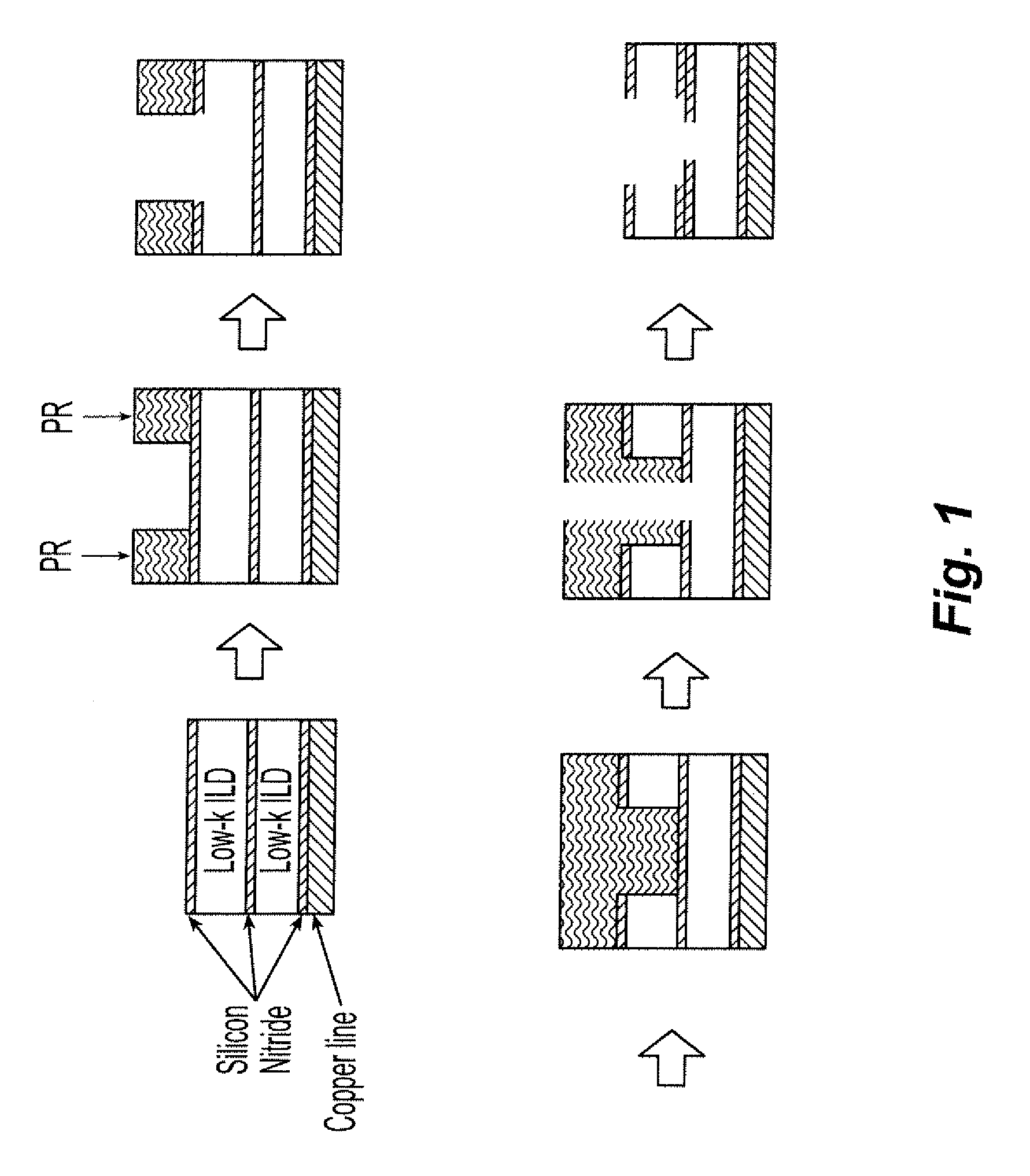
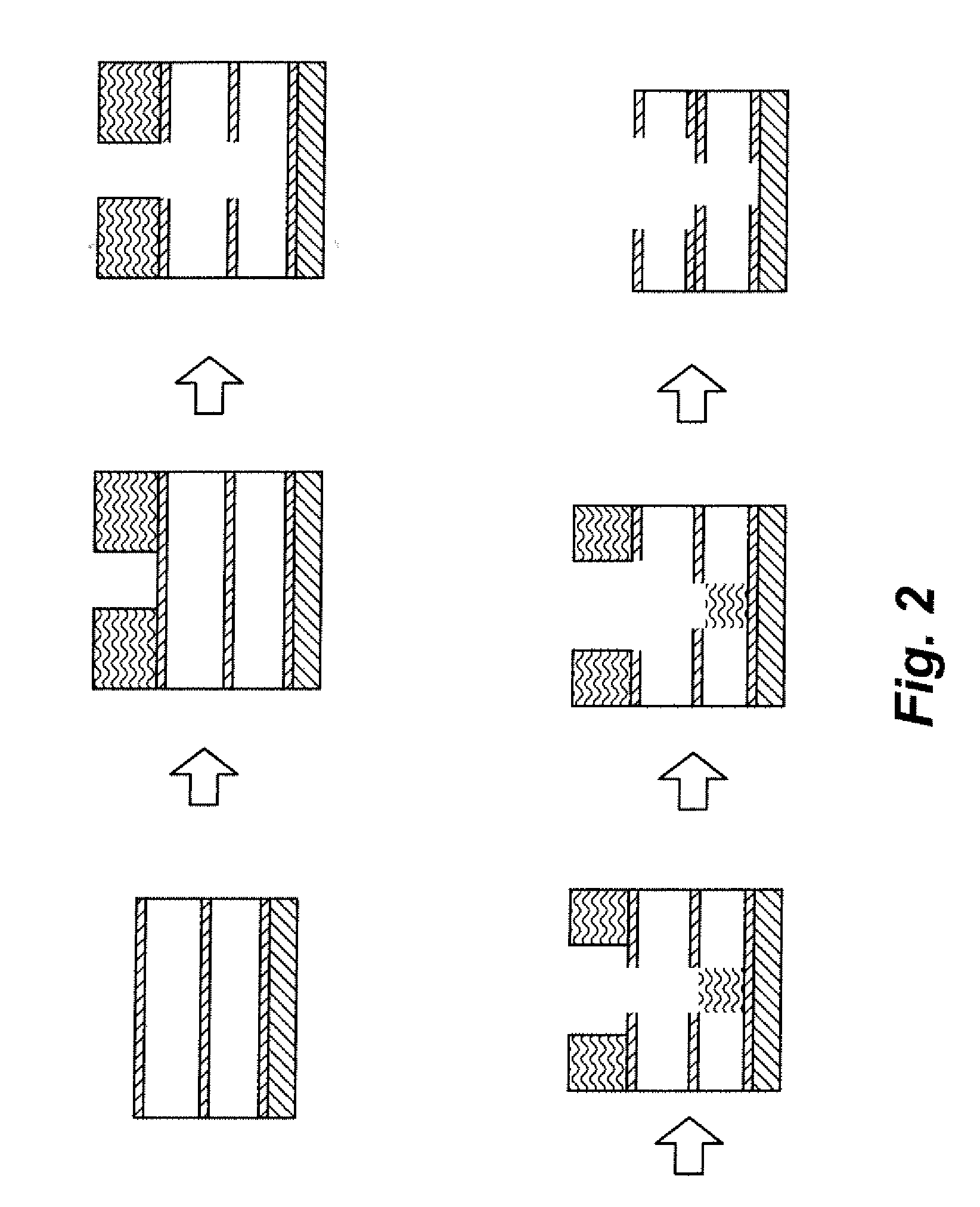
The major drawback of the trench-first approach is that after the trench is etched, the photoresist applied for the via step will completely fill these trenches (see FIG. 1).
Forming the very fine via structures in such strong resist is extremely difficult, and the processing margin for via formation becomes untenable within limited geometries.
The copper will then quickly diffuse into the ILD, causing the failure of the device.
Although the via-first approach has been very successful for dual damascene implementation in silicon dioxide, fluorinated silicate glass (FSG), and some early versions of low-k materials, it faces a severe challenge when used with ultra low-k materials.
However, the highly porous nature of ultra low-k dielectrics may cause further contamination and alteration of its k value because of the absorption of this residual photoresist by the ILD.
This drawback may necessitate the return to a modified trench-first approach to the dual damascene fabrication.
However, even this approach is at risk, because the trench-first approach photoresist pools in the open trench structure prior to via patterning (FIG. 1).
Further problems concerning ultra low-k dielectrics arise with regard to CMP.
However, as the industry drives toward lower and lower ILD k values, the permittivity of silicon nitride (6<k<8) becomes unacceptable.
Its relatively high permittivity undesirably raises the overall permittivity of the ILD stack, compromising the stack's ability to mitigate electrical delay.
This issue is further challenged by the undetermined character of the ILD material to be used for future devices.
In particular, the proliferation of low-k materials is a major obstacle to resolving the dual damascene / low-k integration problem.
Second, the wafer is ashed, exposing the remaining metal.
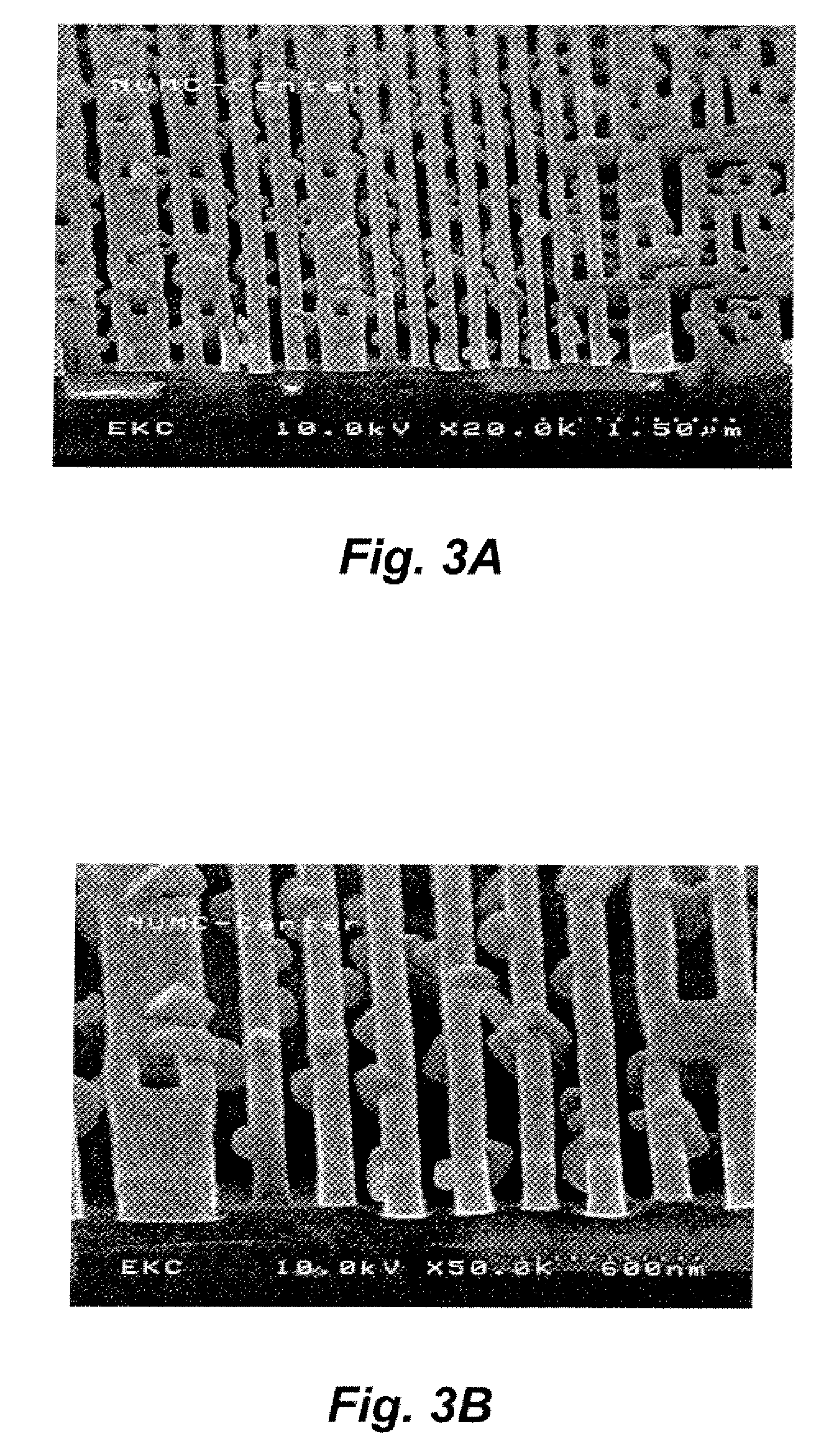
The main challenge of etching a metal hard mask is that the byproducts have a low volatility and the resulting post etch residues are far more difficult to remove than with non-metal hard masks. FIG. 3A and FIG. 3B illustrate the residues remaining on the substrate surface after patterning processes.
During etch and / or ash processing, the low k dielectric materials are damaged by depleting the carbon contents in the low k dielectrics.
Therefore, a simple combination of solvents will often remove resists, though time and temperature constraints in the manufacturing process have in general moved the industry to slightly more aggressive compounds.
Etching residue not removed from the substrate can interfere with subsequent processes involving the substrate.
The effect of poor cleaning results in low device yield, low device reliability, and low device performance.
The substrate is often contaminated from previous process steps with monolayer amounts of metal, anions and / or organic contaminants or surface residues (particles).
However, such formulations are not effective at removing etching residues where a metal hard mask is involved.
However, such formulations are not effective at removing etching residues where a metal hard mask is involved.
However, such formulations are not effective at removing etching residues where a metal hard mask is involved.
Such formulations are also ineffective at removing etching residues where a metal hard mask is involved.
Similarly, such formulations have been found not to be effective where a metal hard mask is involved.
However, such formulations are not effective in removing metal hard mask residues.
Processing conditions are often quite different from one fabrication process to another, making it difficult to apply a particular composition to obtain both effective residue removal and substrate compatibility.
For example, some compositions have produced corrosion on certain metal substrates, such as those including a titanium metal layer.
Used in such a capacity, the layer is often very thin, and corrosion or etching during cleaning operations may compromise the purpose of the layer.
Thus, the quality of the metal interconnection structure filled in the damascene openings is greatly degraded to decrease the yield of product significantly.
This is due to residues from the metal hard mask.
Method used
View moreImage
Smart ImageViewing Examples

Examples
example 1
[0115]A composition 1 for the removal of metal hard mask residue was prepared comprising 0.2 weight percent ammonium bifluoride, 5% maleic acid, 40% DMAC, 54.8% DIW at a pH of 2.62.
example 2
[0116]A composition 2 for the removal of metal hard mask residue was prepared comprising 0.185 weight percent ammonium bifluoride, 32.4% citric acid, 40% DMAC, 54.8% DIW at a pH of 2.62.
example 3
[0117]A composition 3 for the removal of metal hard mask residue was prepared comprising 0.2 weight percent ammonium bifluoride, 25% citric acid, 40% DMAC, 34.8% DIW at a pH of 3.28.
Login to View More PUM
| Property | Measurement | Unit |
|---|---|---|
| pH | aaaaa | aaaaa |
| flash point | aaaaa | aaaaa |
| boiling points | aaaaa | aaaaa |
Abstract
Compositions for removing and cleaning resist, etching residues, planarization residues, metal fluorides and / or metal oxides from a substrate are provided, the composition including a metal ion-free fluoride compound and water. The resist, etching residues, planarization residues, metal fluorides and / or metal oxides are generated during one or more patterning processes during which a metal hard mask is used.
Description
[0001]The present application claims the benefit of U.S. Provisional Application No. 60 / 996,429, filed on Nov. 16, 2007, which is incorporated by reference in its entirety.FIELD OF THE INVENTION[0002]The present invention relates generally to cleaning and etching compositions and a process for removal of residues and contaminants such as polymers, metal oxides, organics and organometallics, and / or metallics, etc. from a semiconductor substrate. More particularly, the present invention relates to the removal of residues using a composition comprising selected fluoride compounds. The invention also relates to a non-corrosive composition useful for the cleaning and etching of many combinations of metals and dielectric compounds. The compositions of the invention are especially useful for cleaning and removing residues in the dual damascene semiconductor manufacturing processes where hard mask layers such as titanium, aluminum, tantalum or alloys such as titanium nitride (TiN), tantalum...
Claims
Login to View More Application Information
Patent Timeline
 Patent Type & AuthorityApplications(United States)
IPC IPC(8): G03F7/42
CPCH01L21/02063H01L21/76813H01L21/76811H01L21/02068
InventorCUI, HUA
OwnerEKC TECH