Method for manufacturing semiconductor device, semiconductor device and electronic appliance

a semiconductor device and electronic appliance technology, applied in the direction of semiconductor devices, basic electric elements, electrical appliances, etc., can solve the problems of single crystal silicon, driver circuit, semiconductor devices which require high speed operation, etc., and achieve excellent driver circuit, reduce the thickness of the semiconductor device, and high speed

Inactive Publication Date: 2009-05-28
SEMICON ENERGY LAB CO LTD
View PDF13 Cites 201 Cited by
  • Summary
  • Abstract
  • Description
  • Claims
  • Application Information

AI Technical Summary

Benefits of technology

[0011]In view of the above-described problem, it is an object of the present invention to provide a method for manufacturing a semiconductor device having a circuit capable of high speed operation at reduced manufacturing cost. It is another object of the present invention to provide a method for manufacturing a semiconductor substrate for providing the semiconductor device and to provide an electronic appliance using the semiconductor device.
[0016]In the above, before formation of the semiconductor element of the pixel region and the semiconductor element of the driver circuit region, by irradiation of the non-single-crystal semiconductor layer and the single crystal semiconductor layer with laser light, the non-single-crystal semiconductor layer may be changed into a microcrystalline semiconductor or a polycrystalline semiconductor and the surface planarity of the single crystal semiconductor layer may be improved.
[0023]By the present invention, a semiconductor element of a circuit region (e.g. a pixel region) which requires a large area can be formed using the non-single-crystal semiconductor layer, and a semiconductor element of a circuit region (e.g. a driver circuit region) which requires high speed operation can be formed using the singe crystal semiconductor layer. Thus, a semiconductor device having an excellent driver circuit can be provided. Further, since the semiconductor device is a device where a driver circuit is integrated, reduction in thickness of the semiconductor device, a reduction in area of a frame region thereof or the like can be realized. Furthermore, since a pixel region can be formed using the non-single-crystal semiconductor layer, the semiconductor device can be made larger very easily.
[0024]Note that in the present invention, by using extremely high planarity of the surface of the non-single-crystal semiconductor layer, a single crystal semiconductor layer is formed over the non-single-crystal semiconductor layer. Therefore, it is not necessary to provide a layer for bonding (attaching) separately, so that manufacturing cost of a semiconductor substrate can be reduced. Here, the single crystal semiconductor layer may be formed so as to be in contact with the non-single-crystal semiconductor layer or may be formed after an insulating layer or the like is formed over the non-single-crystal semiconductor layer.

Problems solved by technology

However, even in a case where microcrystalline silicon or polycrystalline silicon as well as amorphous silicon is used, there is a problem in that characteristics thereof are incomparable to characteristics of single crystal silicon.
In particular, in a semiconductor element which is used for a panel where a driver circuit is integrated, characteristics which are necessary and sufficient (for example, mobility or a subthreshold swing (S value) of a transistor) cannot be obtained.
This has caused a big problem in manufacturing a driver circuit, that is, a semiconductor device which requires high speed operation.

Method used


Image

  • Method for manufacturing semiconductor device, semiconductor device and electronic appliance
  • Method for manufacturing semiconductor device, semiconductor device and electronic appliance
  • Method for manufacturing semiconductor device, semiconductor device and electronic appliance

Examples


embodiment mode 1

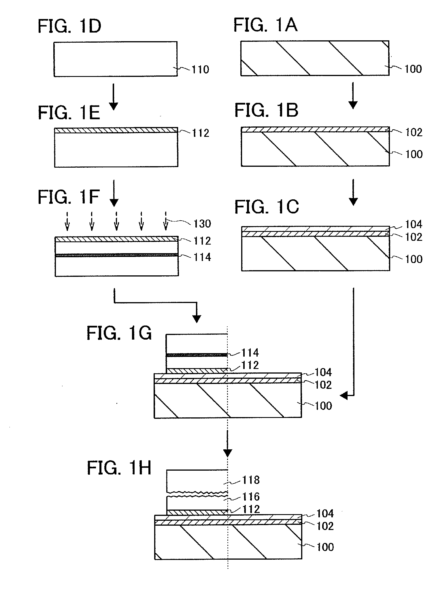
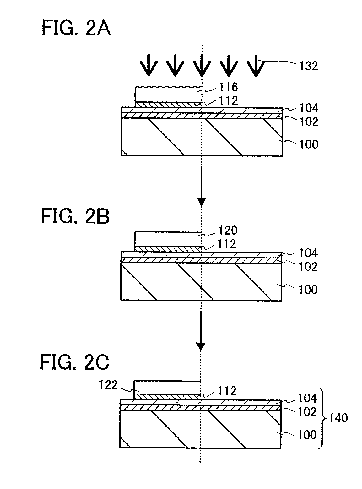
[0056]In this embodiment mode, a method for manufacturing a semiconductor substrate which is used for manufacture of a semiconductor device will be described with reference to FIGS. 1A to 1H, FIGS. 2A to 2C, and FIG. 3.

[0057]First, a base substrate 100 is prepared (see FIG. 1A). As the base substrate 100, a light-transmitting glass substrate used for a liquid crystal display device or the like can be used. As a glass substrate, a substrate having a strain point of greater than or equal to 580° C. and less than or equal to 680° C. (preferably, greater than or equal to 600° C. and less than or equal to 680° C.) may be used. Further, a non-alkali glass substrate is preferable as the glass substrate. As a material of the non-alkali glass substrate, a glass material such as aluminosilicate glass, aluminoborosilicate glass, or barium borosilicate glass is used, for example.

[0058]As the base substrate 100, as well as the glass substrate, a substrate which is formed of an insulator, such as...

embodiment mode 2

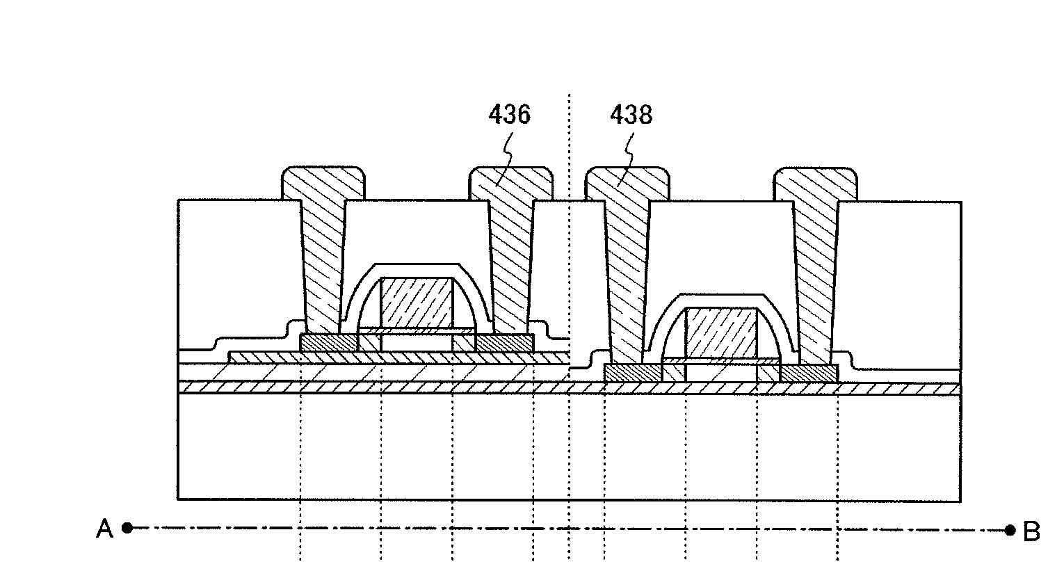
[0138]In this embodiment mode, a method for manufacturing a semiconductor device using the semiconductor substrate manufactured in Embodiment Mode 1 will be described with reference to FIGS. 4A to 4D, FIGS. 5A to 5D and FIGS. 6A and 6B. Here, as an example, a method for manufacturing a semiconductor device including a plurality of transistors will be described.

[0139]FIG. 4A is a cross-sectional view of the semiconductor substrate 140 manufactured in Embodiment Mode 1.

[0140]An impurity element imparting p-type conductivity such as boron, aluminum, or gallium or an impurity element imparting n-type conductivity such as phosphorus, or arsenic may be added to a non-single-crystal semiconductor layer 104 and a single crystal semiconductor layer 122 in order to control a threshold voltage of a transistor. A region to which the impurity element is added and the kind of the impurity element to be added can be changed as appropriate. For example, an impurity element imparting p-type conducti...

embodiment mode 3

[0174]In this embodiment mode, another example of a method for manufacturing a semiconductor substrate will be described with reference to FIGS. 7A to 7I and FIGS. 8A to 8C.

[0175]First, a base substrate 100 is prepared (see FIG. 7A). A detailed description of the base substrate 100 is omitted here because Embodiment Mode 1 can be referred to therefor.

[0176]Next, an insulating layer 102 is formed over a surface of the base substrate 100 (see FIG. 7B). The insulating layer 102 may have a single layer structure or a stacked layer structure. Embodiment Mode 1 can be referred to for a detailed description of a material or the like for the insulating layer 102. It is possible to employ a structure in which the insulating layer 102 is not formed; however, when a substrate including an impurity which decreases the reliability of a semiconductor device, such as alkali metal or alkaline earth metal, is used as the base substrate 100, the insulating layer 102 is preferably provided so that suc...


PUM


Abstract

A non-single-crystal semiconductor layer is formed over a substrate, and then a single crystal semiconductor layer is formed over part of the non-single-crystal semiconductor layer. Thus, a semiconductor element of a region which requires a large area (e.g. a pixel region in a display device) can be formed using the non-single-crystal semiconductor layer, and a semiconductor element of a region which requires high speed operation (e.g. a driver circuit region in a display device) can be formed using the single crystal semiconductor layer.

Description

BACKGROUND OF THE INVENTION[0001]1. Field of the Invention[0002]The present invention relates to a method for manufacturing a semiconductor device, a semiconductor device and an electronic appliance.[0003]2. Description of the Related Art[0004]In recent years, flat panel displays such as liquid crystal display devices and electroluminescence (EL) display devices have attracted attention.[0005]Driving methods of the flat panel displays include a passive matrix method and an active matrix method. An active matrix method has advantages over a passive matrix method in low power consumption, high definition, a large-sized substrate, and the like.[0006]Here, a structural example of an active matrix panel is briefly described with reference to FIGS. 21A and 21B. FIG. 21A illustrates an example of a structure in which a driver circuit is provided using a tape automated bonding (TAB) method.[0007]In FIG. 21A, a pixel portion 2101 in which pixels 2102 are arranged in matrix is formed over a s...

Claims


Application Information

Patent Timeline
Patent Type & Authority Applications(United States)
IPC IPC(8): H01L29/04H01L21/336
CPCH01L27/1214H01L29/66772H01L27/1266H01L21/76254
Inventor YOKOI, TOMOKAZUSAKURADA, YUJIRO
Owner SEMICON ENERGY LAB CO LTD
Why Eureka
Try Eureka