

Tellurium Precursors for GST Films in an ALD or CVD Process
a technology of gst films and precursors, which is applied in the field of gst film precursors in an ald or cvd process, can solve the problems of high reset current needs to be applied, difficult to fill plugs or high aspect ratio holes with gst materials, and difficult to form thin layers of gst materials
- Summary
- Abstract
- Description
- Claims
- Application Information
AI Technical Summary
Problems solved by technology
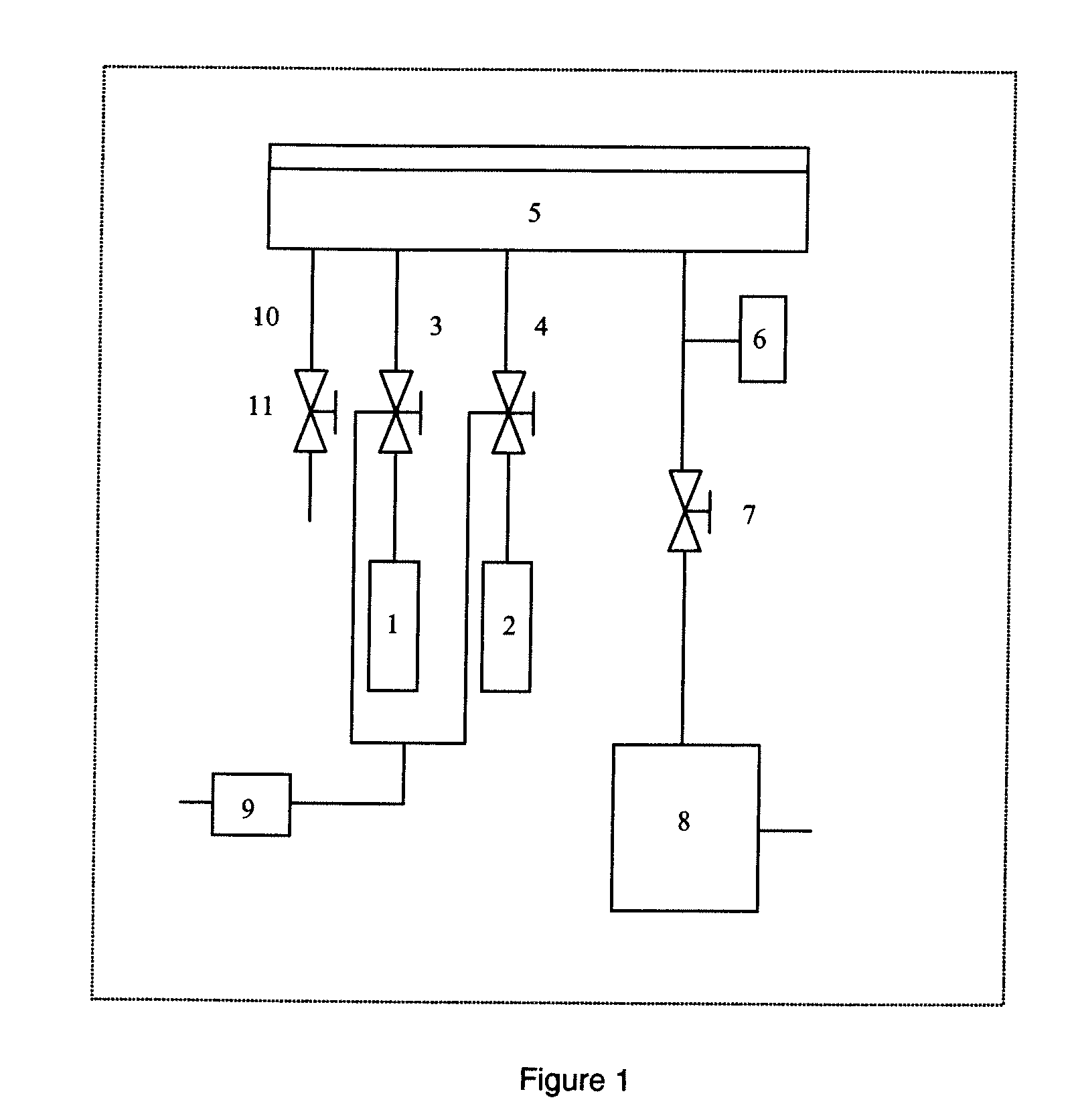
Method used
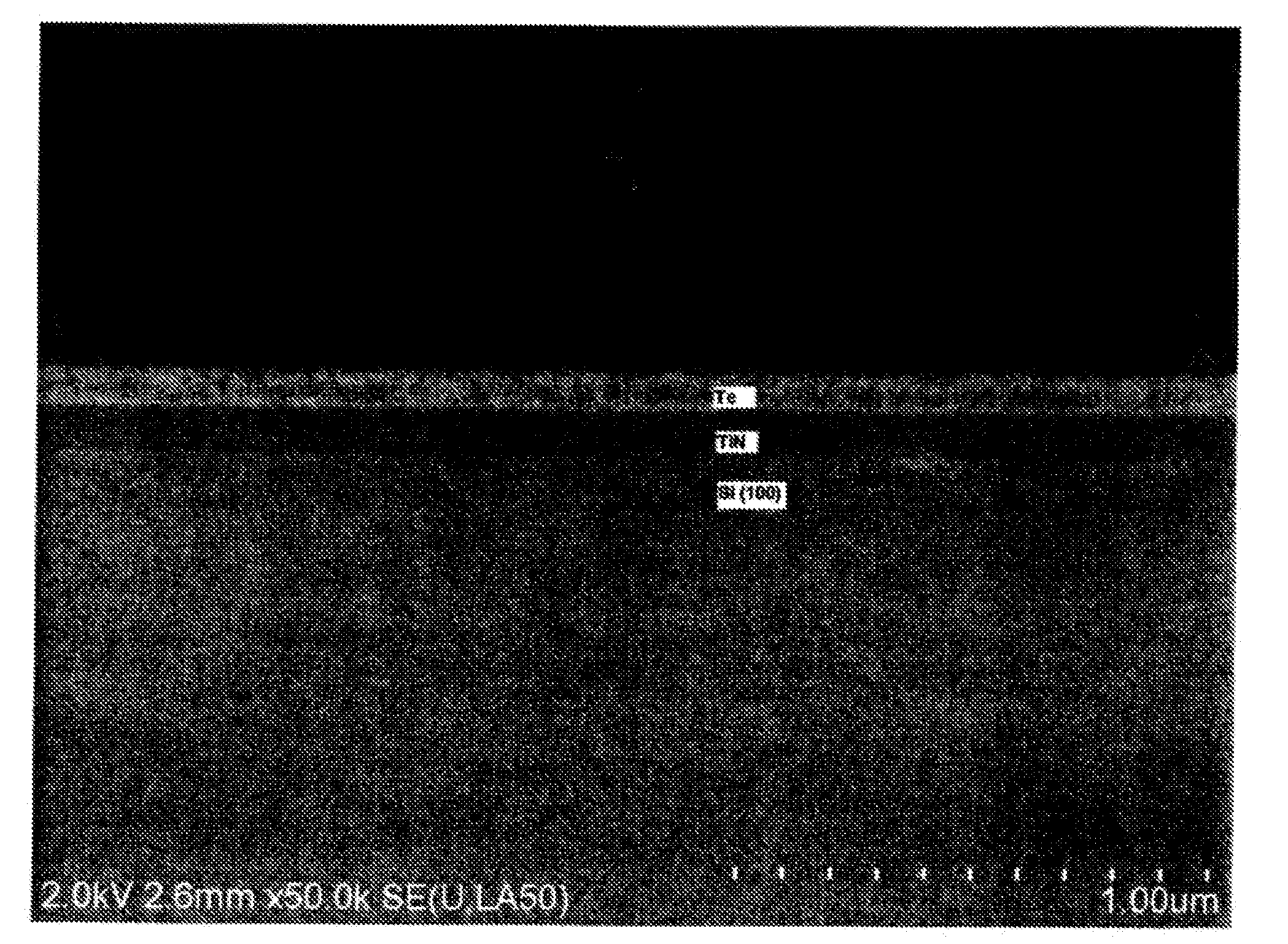
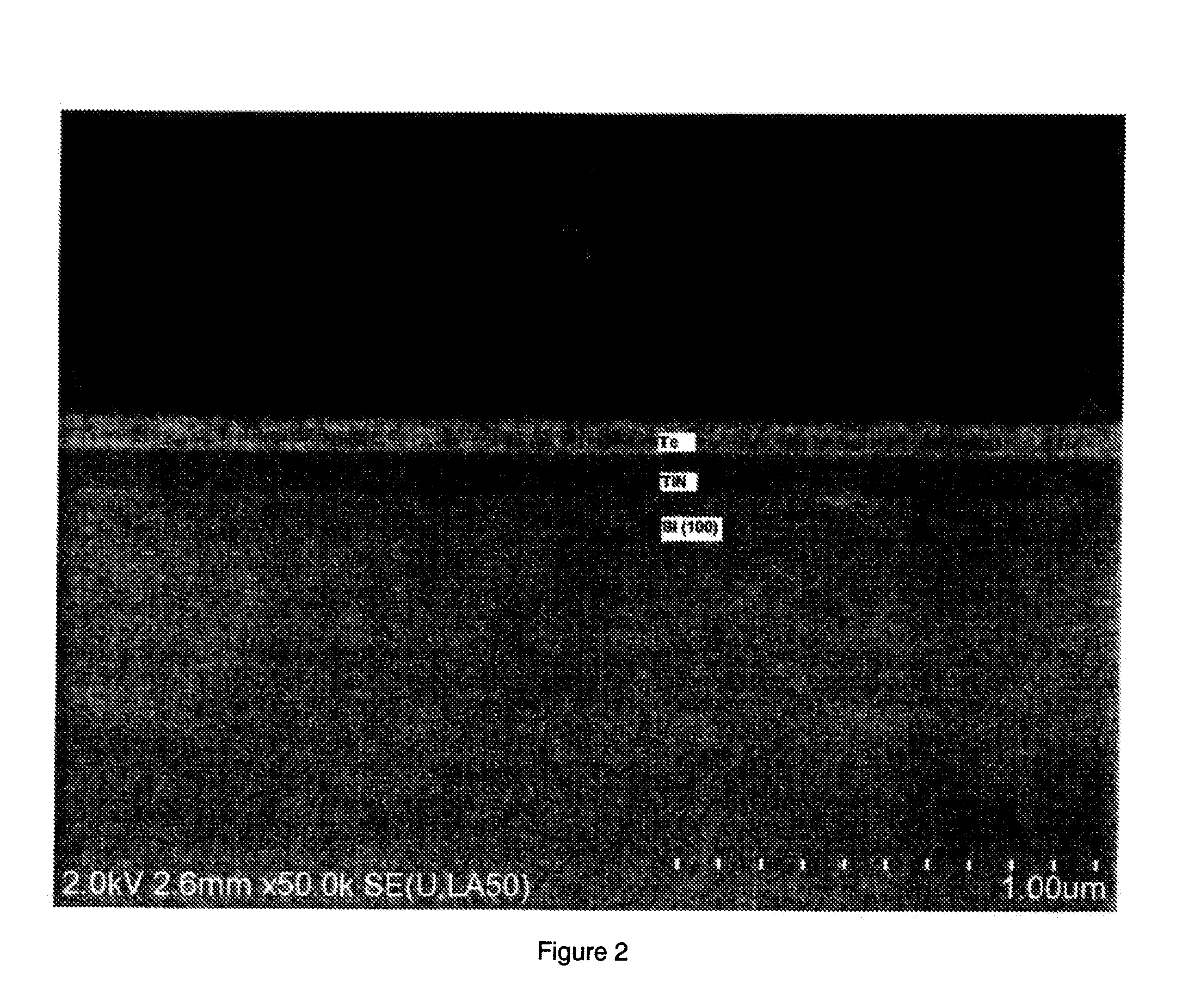
Image

Examples
example 1
Synthesis of Hexamethyldisilyltellurium
[0064]1.28 g (0.01 mol) 200 mesh tellurium powder, 0.48 g (0.02 mol) lithium hydride, and 40 ml tetrahydrofuran (THF) were placed in a 100 ml flask. With stirring, the mixture was refluxed for 4 hours. All black powder of tellurium disappeared, and a muddy color precipitate was formed. Then, the mixture was cooled down to −20° C.; 2.2 g (0.02 mol) trimethylchlorosilane was added. The mixture was allowed to warm up to room temperature. After stirring for 4 hours, the mixture was filtered under inert atmosphere. The solvent was removed by distillation. Hexamethyldisilyltellurium was purified by vacuum distillation, b.p. 50° C. at 2.5 mmHg.
example 2
Synthesis of Tetramethyldisilyltellurium
[0065]3.84 g (0.03 mol) 200 mesh tellurium powder, 1.38 g (0.06 mol) sodium, 0.77 h (0.006 mol) naphthalene, and 50 ml THF were placed in a 100 ml flask. The mixture was stirred at room temperature for 24 hours. All black powder of tellurium and sodium disappeared, and a muddy color precipitate was formed. Then, the mixture was cooled down to −20° C.; 5.77 g (0.06 mol) dimethylchlorosilane was added. The mixture was allowed to warm up to room temperature. After stirring for 4 hours, the mixture was filtered under inert atmosphere. The solvent was removed by distillation. Tetramethyldisilyltellurium was purified by vacuum distillation, B.P. 50° C. at 4 mmHg.
example 3
Synthesis of Trimethylsilyl-t-butyltellurium
[0066]6.4 g (0.05 mol) 200 mesh tellurium powder, 100 ml diethyl ether, and 20 ml 2.5 M t-butyllithium in hexane were added to a 250 ml flask. At 0° C., the mixture was stirred for 8 hours. All black powder of tellurium disappeared, and a muddy color precipitate was formed. To this mixture, 5.4 g (0.05 mol) trimethylchlorosilane was added. The mixture was allowed to warm up to room temperature. After stirring for 1 hour, the mixture was filtered under inert atmosphere. The solvent was removed by distillation. Trimethylsilyl-t-butyltellurium was purified by vacuum distillation.
PUM
| Property | Measurement | Unit |
|---|---|---|
| temperature | aaaaa | aaaaa |
| temperature | aaaaa | aaaaa |
| semiconductor | aaaaa | aaaaa |
Abstract
Description
Claims
Application Information