

Photovoltaic Device with Solution-processed Chalcogenide Absorber Layer
a photovoltaic device and absorber layer technology, applied in the field of photovoltaic devices, can solve the problems of insufficient incremental improvement in existing energy technologies to meet the demand, the cost of fabricating a high-performance thin-film, and the fact that less than 0.1% of the world's electricity is generated by solar electricity generation, etc., to achieve the effect of improving electrical characteristics and reducing costs
- Summary
- Abstract
- Description
- Claims
- Application Information
AI Technical Summary
Benefits of technology
Problems solved by technology
Method used
Image

Examples
example 1
[0133]The solutions used for the thin-film deposition were prepared in an inert atmosphere in two steps. First, solutions for each of the individual component metal chalcogenides were prepared, all at room temperature, and then the component solutions were mixed in the appropriate ratios to yield a stoichiometric solution for the targeted overall CIGS composition.
[0134]Component solution (a) contained 4 mmol In2Se3 (1.886 g) and 4 mmol Se (0.316 g) dissolved in 12 mL of anhydrous hydrazine. After several days a clear pale yellow and very viscous solution formed. Solution (b) contained 1.5 mmol Ga (0.105 g; ground up) and 3 mmol of Se (0.237 g) dissolved in 3 mL of anhydrous hydrazine (after a week of stirring). Solution (c) contained 4 mmol Cu2S (0.637 g) and 8 mmol S (0.256 g) dissolved in 8 mL of anhydrous hydrazine, forming a clear yellow solution. Solution (d) contained 4 mmol Se (0.316 g) dissolved in 2 mL of hydrazine.
[0135]From these initial component solutions, 3 CIGS soluti...
example 2
[0163]Grain structure control is achieved using a small amount of included Sb doping (from CuSbS2). The solutions used for the film depositions were prepared in a similar fashion to that described in example 1, with the exception of mixing in a small quantity (2 solutions during the second step. In addition, the example here considers CuInSe2 as the target system instead of Cu(In,Ga)Se2. However, similar effects of Sb-inclusion on grain structure for the Ga-containing system has also been observed.
[0164]Component solution (a) containing 3 mmol In2Se3 (1.3996 g) and 3 mmol Se (0.237 g) dissolved in 9 mL of anhydrous hydrazine. After several days, a clear pale yellow and very viscous solution formed. Solution (b) contained 4 mmol Cu2S (0.637 g) and 8 mmol S (0.256 g) dissolved in 8 mL of anhydrous hydrazine, forming a clear yellow solution. Solution (c) contained 4 mmol Se (0.316 g) dissolved in 2 mL of hydrazine. Solution (d) c contained 4 mmol Sb2S3 (1.359 g) and 8 mmol S (0.256 g) ...
example 3
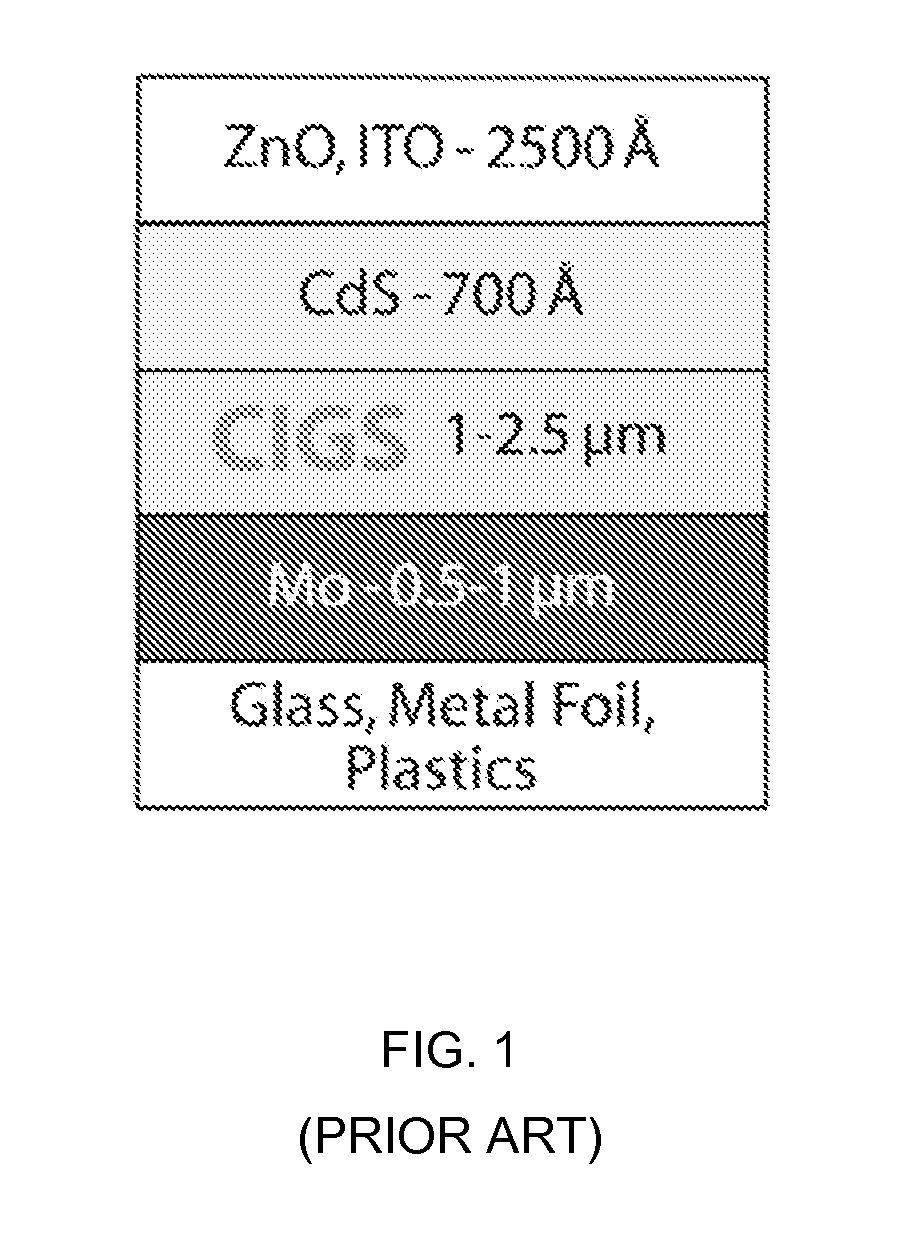
[0189]The CIGS absorber layers described above were incorporated into a working PV device of the general structure outlined in FIG. 1, with, however, the CIGS absorber layer deposited using the method of the present invention.
[0190]A 1″×1″ soda-lime glass plate (0.04″ thickness) with about 900 nm of Mo sputtered on top formed the back contact of the device.
[0191]For each component solution, the solid components were weighed and the solutions were formed in a nitrogen-filled glove box with water and oxygen levels maintained below 1 ppm.
[0192]The component solutions for the CIGS layer were formed as follows:
[0193]Solution A (Cu2S) was formed by mixing 6 mmol Cu2S (0.955 g), 12 mmol S (0.3848 g) and 12.0 mL of anhydrous hydrazine (Aldrich, anhydrous, 98%), leading to a clear yellow solution after several days of stirring.
[0194]Solution B (In2Se3) was formed by mixing 4 mmol In2Se3 (1.8661 g), 4 mmol Se (0.3158 g) and 12.0 mL hydrazine (Aldrich, anhydrous, 98%), yielding a viscous pale ...
PUM
 Abstract
Description
Claims
Application Information