Semiconductor laser device and method for manufacturing the same

a laser device and semiconductor technology, applied in the field of semiconductor lasers, can solve the problems of difficult to secure a sufficiently large selectivity, difficult to solve the ridge shape asymmetry, and difficulty in achieving sufficient difference in etching speed between materials, so as to improve differential quantum efficiency, improve element characteristics, and improve the effect of horizontal radiation angl

Active Publication Date: 2009-06-11
PANASONIC SEMICON SOLUTIONS CO LTD
View PDF6 Cites 6 Cited by
  • Summary
  • Abstract
  • Description
  • Claims
  • Application Information

AI Technical Summary

Benefits of technology

[0075]According to the present invention described above, it is possible to provide a ridge stripe semiconductor laser device that achieves improved element characteristics such as a uniform horizontal radiation angle of a laser beam, an improved differential quantum efficiency and an improved kink level, and a method for manufacturing the same. Further, a ridge-shaped stripe can be formed with excellent uniformity on a wafer surface and between wafers, thus allowing a yield improvement.

Problems solved by technology

From the above, it has been very difficult to solve the asymmetry of the ridge shape and improve the perpendicularity thereof in the cross-section perpendicular to the longitudinal direction (stripe direction) of the ridge.
In dry etching, since sputtering, which is a physical phenomenon, is a prime factor, it is difficult to secure a sufficiently large selectivity such as that achieving a sufficient difference in an etching speed between materials.

Method used


Image

  • Semiconductor laser device and method for manufacturing the same
  • Semiconductor laser device and method for manufacturing the same
  • Semiconductor laser device and method for manufacturing the same

Examples


embodiment 1

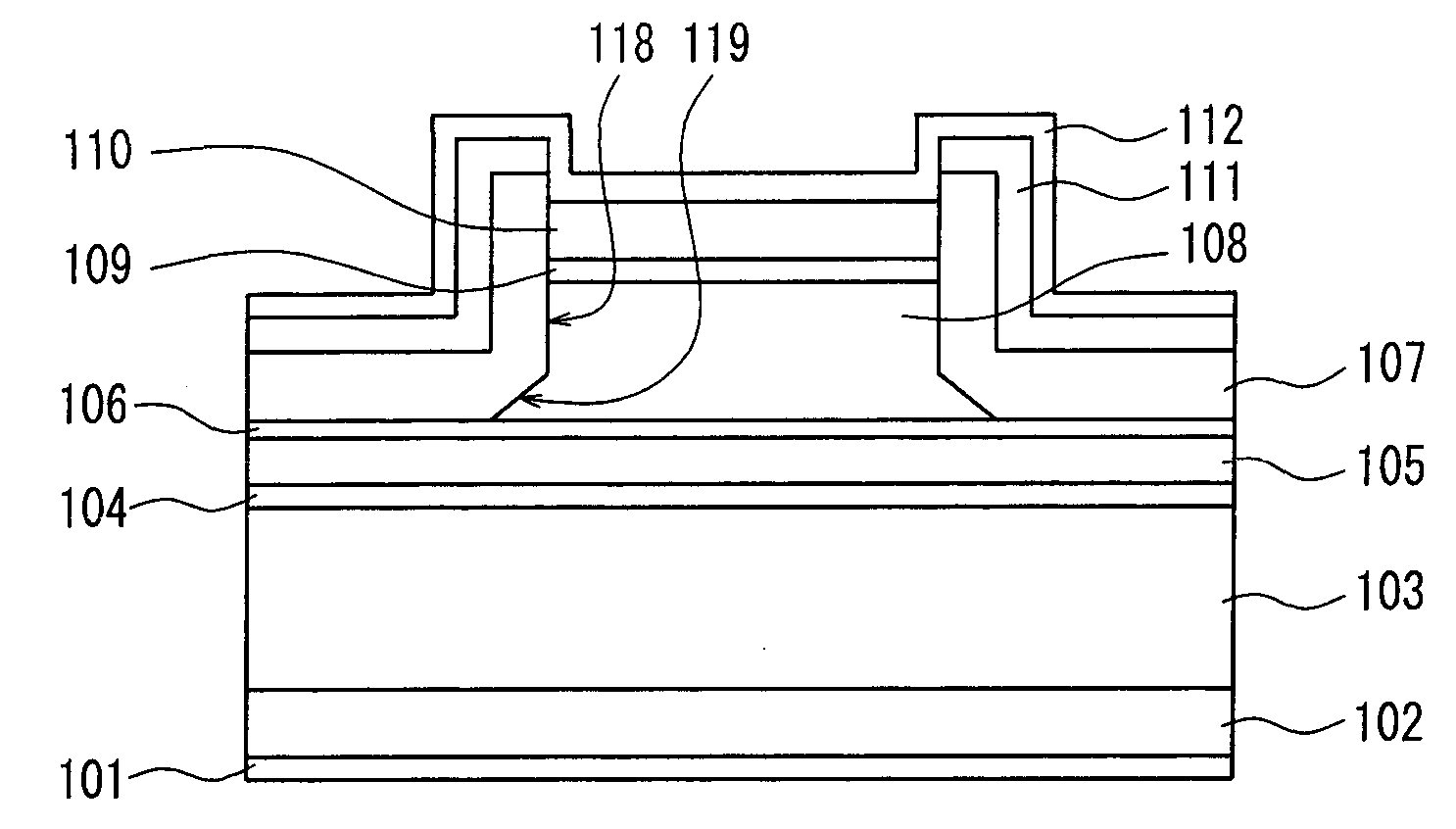
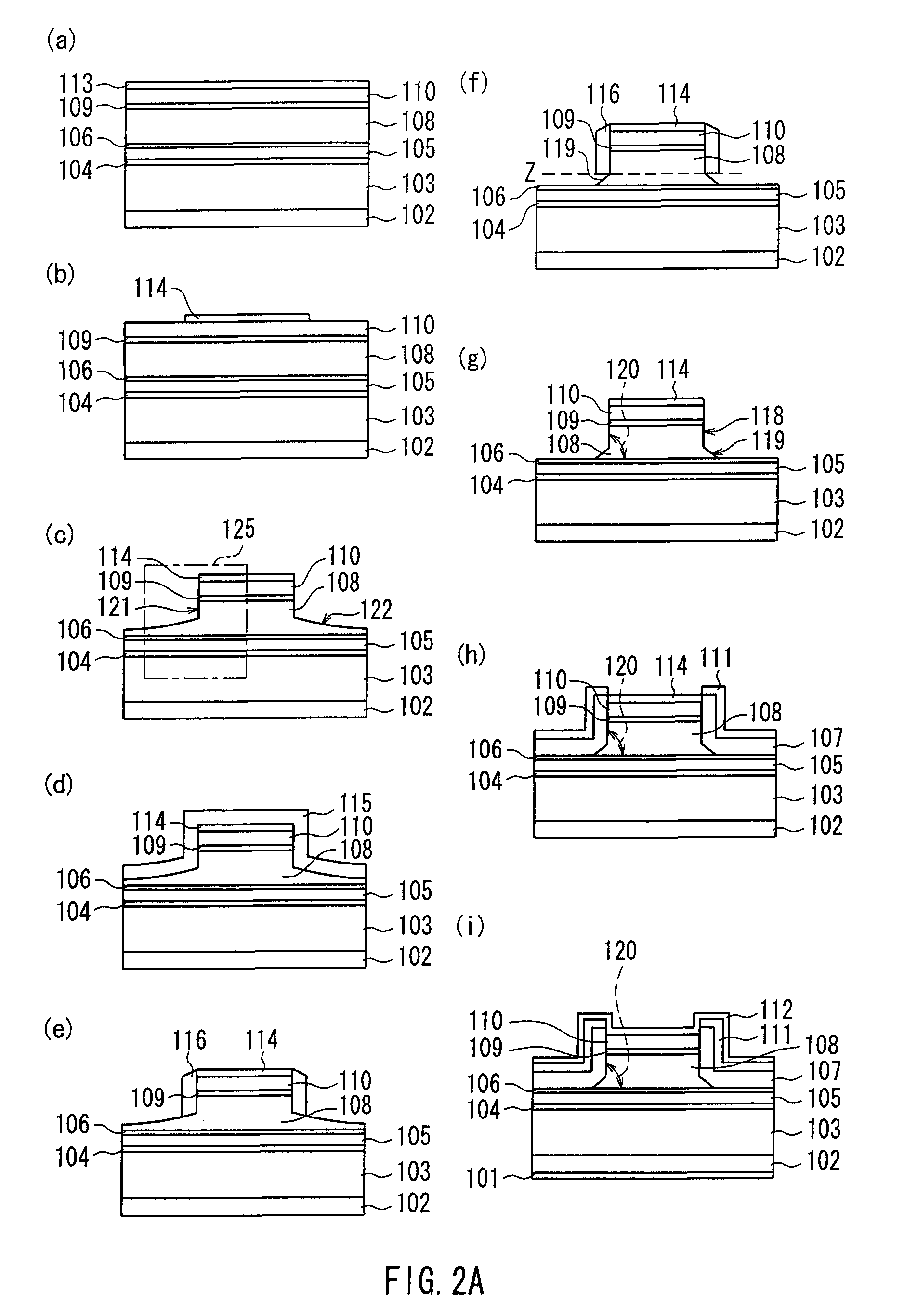
[0181]FIG. 1 is a sectional view showing a ridge stripe semiconductor laser device in Embodiment 1 of the present invention taken along a direction perpendicular to a stripe longitudinal direction of the ridge, and FIG. 2A is a sectional view showing manufacturing processes of the same. In the description of the semiconductor laser device in the present invention, upward / downward and an upper side / a lower side of the semiconductor laser device are defined as follows: referring to FIG. 1, for example, a side on which an n-side electrode 101 is present is called downward or a lower side, and a side on which a p-side electrode 112 is present is called upward or an upper side. A similar definition applies to other figures. Upward in each figure is called upward or an upper side in the description of the semiconductor laser device, and downward in each figure is called downward or a lower side. Further, unless otherwise specified, the other figures are all sectional views taken along the...

embodiment 2

[0230]FIGS. 2E and 2F are sectional views showing manufacturing processes of a ridge stripe semiconductor laser device in Embodiment 2. Embodiment 2 aims at suppressing the changes in a refractive index due to the steps 117 described above and forming the dimension and shape of the ridge stably. Since Embodiment 2 has the processes up to forming the SiO2 stripe 114 as shown in FIG. 2A(b) in common with Embodiment 1, only the processes thereafter will be described here. Also, the present embodiment has the configuration of the layers in common with Embodiment 1.

[0231]After forming the SiO2 stripe 114, the p-type (Al0.7Ga0.3)0.5In0.5P second cladding layer 108, the p-type Ga0.5In0.5P intermediate layer 109 and the p-type GaAs contact layer 110 are dry-etched midway through the p-type (Al0.7Ga0.3)0.5In0.5P second cladding layer 108 using the SiO2 stripe 114 as a mask in order to suppress the formation of a refractive index step caused by the step 117. At this time, the ridge shape gene...

embodiment 3

[0269]FIGS. 2K(w-1) to (w-6) and 2K(x) are sectional views showing manufacturing processes of a ridge stripe semiconductor laser device in Embodiment 3. Embodiment 3 is limited to the case of using a semiconductor substrate in which the n-type GaAs substrate 102 is off-angled such that its substrate orientation is tilted from a (100) plane in a direction. As described in Embodiment 1, when an off-angled substrate is used, the intermediate step surfaces 117 always are formed as shown in FIGS. 2B(l), (m), (n) and 2C(p), for example. Accordingly, by suppressing the formation of the intermediate step surfaces 117 in Embodiment 1, Embodiment 3 aims at suppressing the change in the refractive index generated near a connection portion of the intermediate step surfaces 117 and the second surfaces 119 and further forming the ridge with excellent dimension controllability and reproducibility. Since Embodiment 3 has the processes up to forming the lateral wall protective layer 116 as shown in ...


PUM


Abstract

A ridge stripe type semiconductor laser device is provided, on a semiconductor substrate (102), with a first conduction type cladding layer (103), an active layer (104), a second conduction type first cladding layer (105), a second conduction type second cladding layer (108) of a ridge type stripe shape for confining direction, and a current block layer (107) formed by removing at least an upper portion of the ridge. In a section normal to the stripe direction of the ridge, each of the two side faces of the ridge is provided with a first face (118) substantially normal to the semiconductor substrate surface and extending downward from the upper end of the ridge, and a second face (119) formed to have a substantially straight skirt slope face inclined at the ridge skirt portion obliquely downward to the ridge outside. The first face and the second face are made to merge either directly or through a third intermediate face into each other. A face (111) of a semiconductor constituting the second cladding layer is exposed to the second face. The semiconductor laser device thus provided can have a high kink level and a high output with a low operating current.

Description

TECHNICAL FIELD[0001]The present invention relates to a semiconductor laser device used as a light source in an optical disk apparatus, an information processing apparatus or the like, and a method for manufacturing the same.BACKGROUND ART[0002]Accompanying higher density recording in optical disks such as DVDs, not only DVD drives for reproduction but also DVD drives for recording information in DVD-RAMs, DVD-RW or the like have become commercialized. Also, their recording speed keeps increasing.[0003]In response to such an increasing recording speed of the DVD drives for recording, there has been a demand for higher power semiconductor lasers used as their light source. As an effective means of achieving the higher power of semiconductor lasers, various suggestions have been made; one of which is to process a cladding layer above an active layer, thus forming a ridge-shaped stripe having high perpendicularity and high symmetry. Incidentally, having high perpendicularity and high s...

Claims


Application Information

Patent Timeline
Patent Type & Authority Applications(United States)
IPC IPC(8): H01S5/22H01L21/70
CPCH01S5/223
Inventor HOSOI, HIROYUKIMAKITA, KOUJIYAMANAKA, MICHINARI
Owner PANASONIC SEMICON SOLUTIONS CO LTD
Why Eureka
Try Eureka