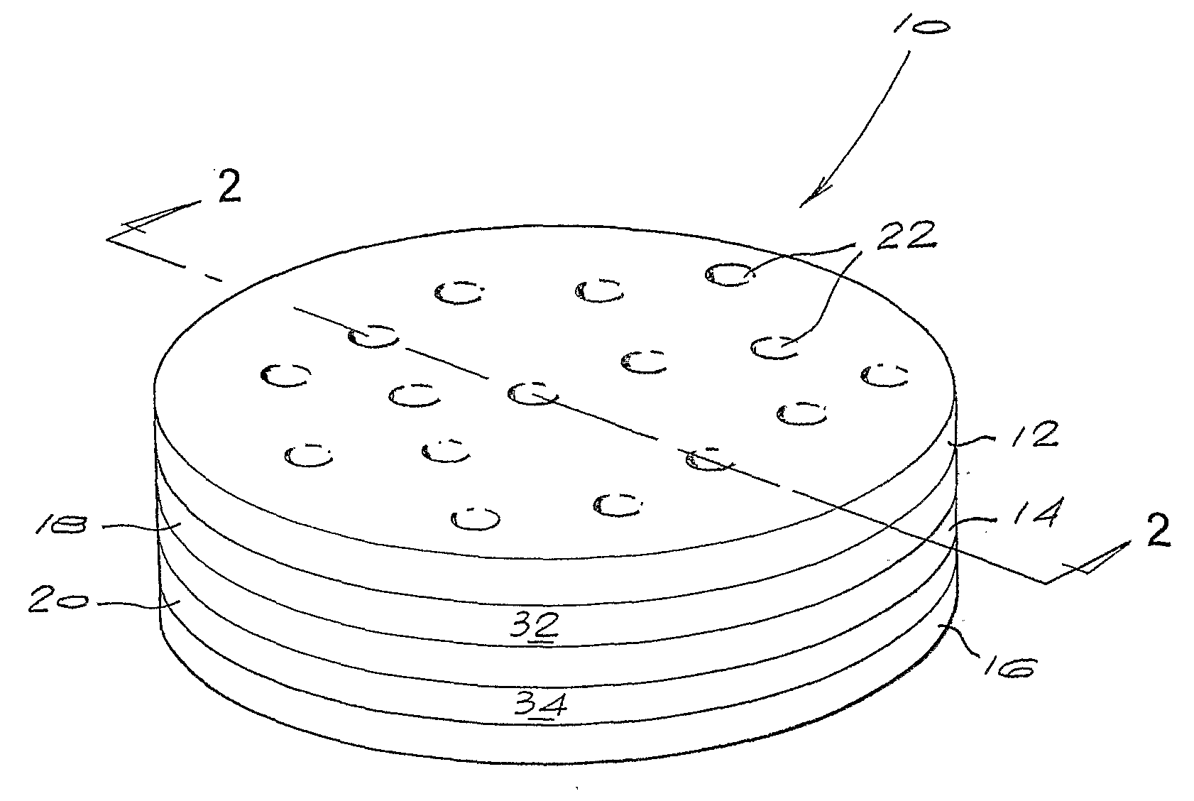
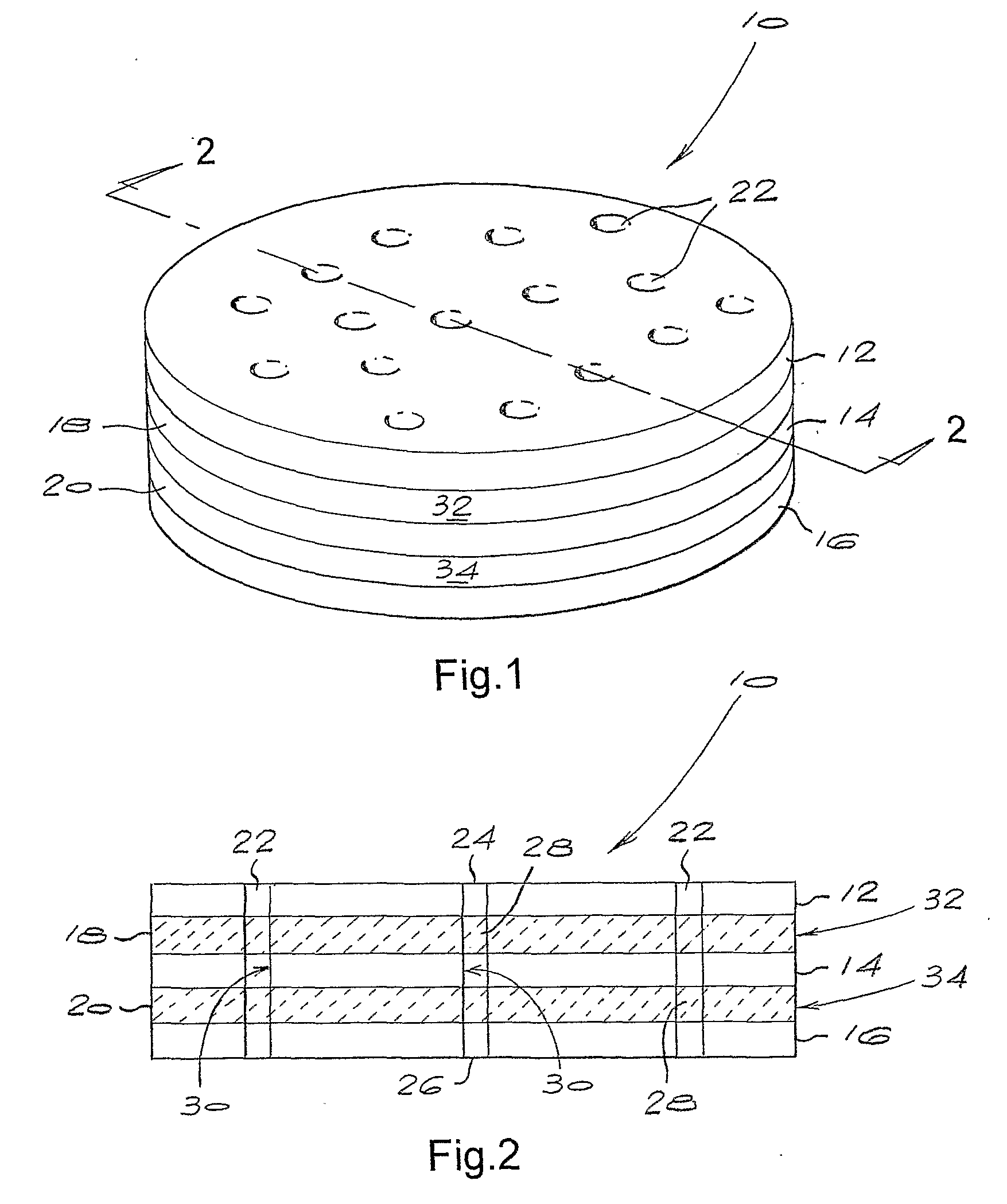
Microelectrode array
a technology of microelectrodes and arrays, applied in the field of microelectrodes, can solve the problems of complex method of device fabrication, and achieve the effect of facilitating fabrication
- Summary
- Abstract
- Description
- Claims
- Application Information
AI Technical Summary
Benefits of technology
Problems solved by technology
Method used
Image

Examples
example 1
[0146]The route for the fabrication of the diamond microelectrode of the first embodiment of the invention is shown in FIG. 5.
[0147]A plate of intrinsic polycrystalline diamond about 500 μm thick and 24 mm in diameter was prepared. The growth surface of the plate was mechanically processed to a surface roughness Ra of less 100 nm by lapping. The nucleation surface was in the as-grown state and had a surface roughness Ra of less than 1 μm. After preparing the surface, the plate was cleaned using a hot oxidising mixture of concentrated sulphuric acid and potassium nitrate at a temperature greater that 150° C.
[0148]The plate was placed inside chemical vapour deposition (CVD) system capable of depositing boron-doped diamond. A layer of boron doped diamond about 140 μm thick was deposited onto the growth surface. The deposition conditions were chosen to provide a boron concentration in the deposited layer of between about 2×10²⁰ atoms per cm3 (about 1000 ppm) and about 1×10²¹ atoms per c...
example 2
[0151]A plate consisting of an intrinsic diamond layer, a boron doped diamond layer and a further intrinsic layer was prepared as in Example 1. After the lapping and cleaning stage, a further layer of boron doped diamond (“second boron-doped diamond layer”) about 140 μm thick was deposited on to one of the surface. After deposition, the surface of the second boron doped diamond layer was lapped to a surface roughness Ra of less than 100 nm and thickness of about 100 μm. After a further cleaning step using the hot oxidising mixture of concentrated sulphuric acid and potassium nitrate at a temperature greater that 150° C., a further intrinsic diamond layer, about 250 μm thick, was deposited on top of the second boron doped diamond layer. This layer was lapped to a surface roughness Ra of less than 100 nm and a thickness of about 200 μm.
[0152]The synthesised stack of diamond layers thus comprised:[0153]an intrinsic diamond layer about 500 μm thick,[0154]a boron-doped diamond layer abou...
example 3
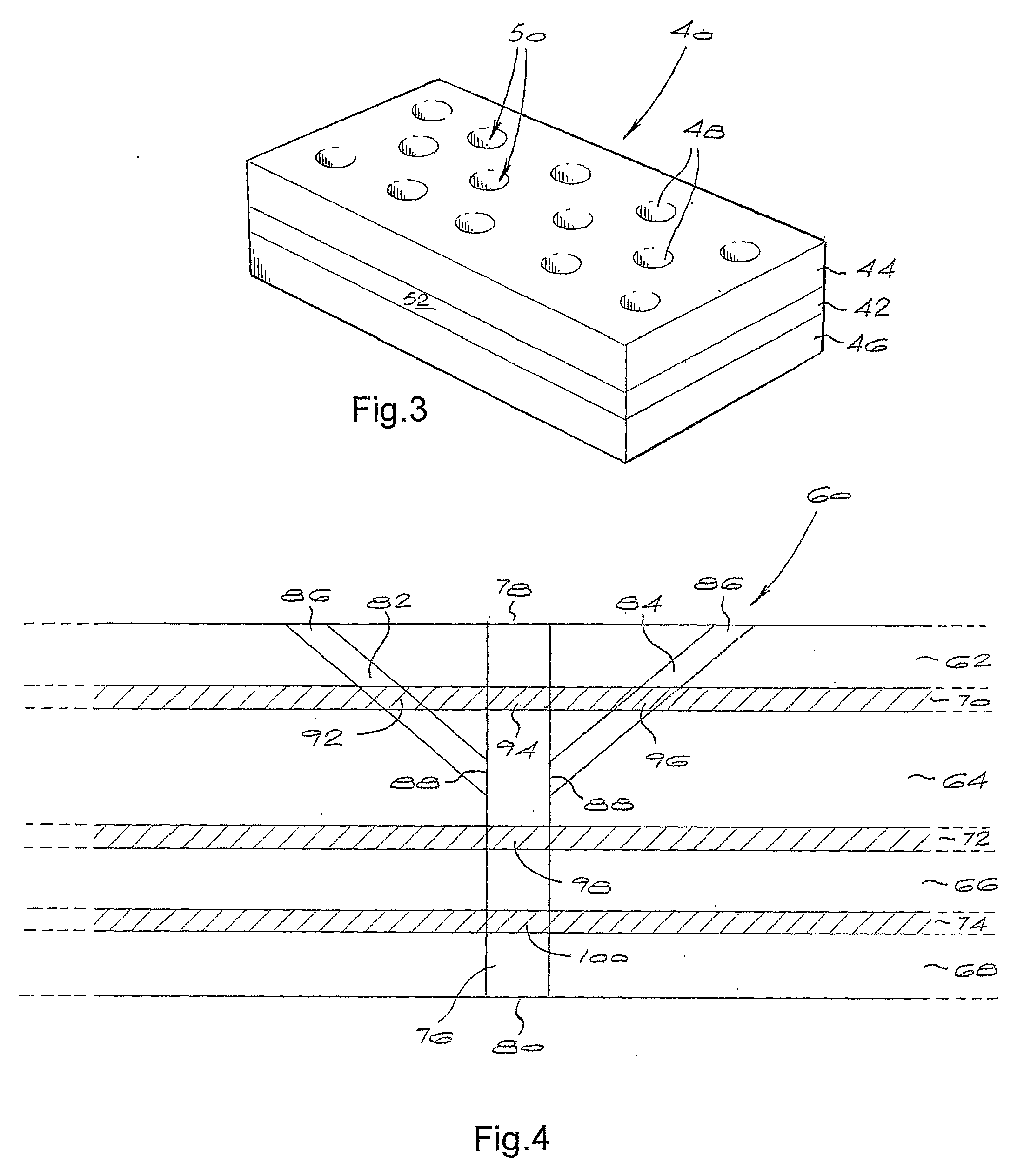
[0161]A schematic perspective view of the third embodiment of the diamond microelectrode of the invention is shown in FIG. 6 and a route for its fabrication is shown in FIG. 7.
[0162]A plate of intrinsic polycrystalline diamond about 500 μm thick and 24 mm in diameter was prepared. The growth surface of the plate was mechanically processed to a surface roughness Ra of less 100 nm by lapping. The nucleation surface was in the as-grown state and had a surface roughness Ra of less than 1 μm. After preparing the surface, the plate was cleaned using a hot oxidising mixture of concentrated sulphuric acid and potassium nitrate at a temperature greater that 150° C.
[0163]The plate was placed inside chemical vapour deposition (CVD) system capable of depositing boron doped diamond. A layer of boron doped diamond about 140 μm thick was deposited onto the growth surface. The deposition conditions were chosen to provide a boron concentration in the deposited layer of between about 2×10²⁰ atoms per...
PUM
| Property | Measurement | Unit |
|---|---|---|
| thickness | aaaaa | aaaaa |
| total thickness | aaaaa | aaaaa |
| diameter | aaaaa | aaaaa |
Abstract
Description
Claims
Application Information
 - Generate Ideas
- Intellectual Property
- Life Sciences
- Materials
- Tech Scout
- Unparalleled Data Quality
- Higher Quality Content
- 60% Fewer Hallucinations
Browse by: Latest US Patents, China's latest patents, Technical Efficacy Thesaurus, Application Domain, Technology Topic, Popular Technical Reports.
© 2025 PatSnap. All rights reserved.Legal|Privacy policy|Modern Slavery Act Transparency Statement|Sitemap|About US| Contact US: help@patsnap.com