

Nitride semiconductor substrate and method of producing same
a technology of nitride and semiconductor substrate, which is applied in the direction of crystal growth process, polycrystalline material growth, chemically reactive gas growth, etc., can solve the problems of reducing the random facet growth method, preventing device makers from making a plurality of equivalent devices, and reducing the dislocation of neighboring single crystal regions , the effect of convenient device fabrication
- Summary
- Abstract
- Description
- Claims
- Application Information
AI Technical Summary
Benefits of technology
Problems solved by technology
Method used
Image

Examples
embodiment 1
Sapphire Template Undersubstrate; Patterns A-J; FIGS. 11-15
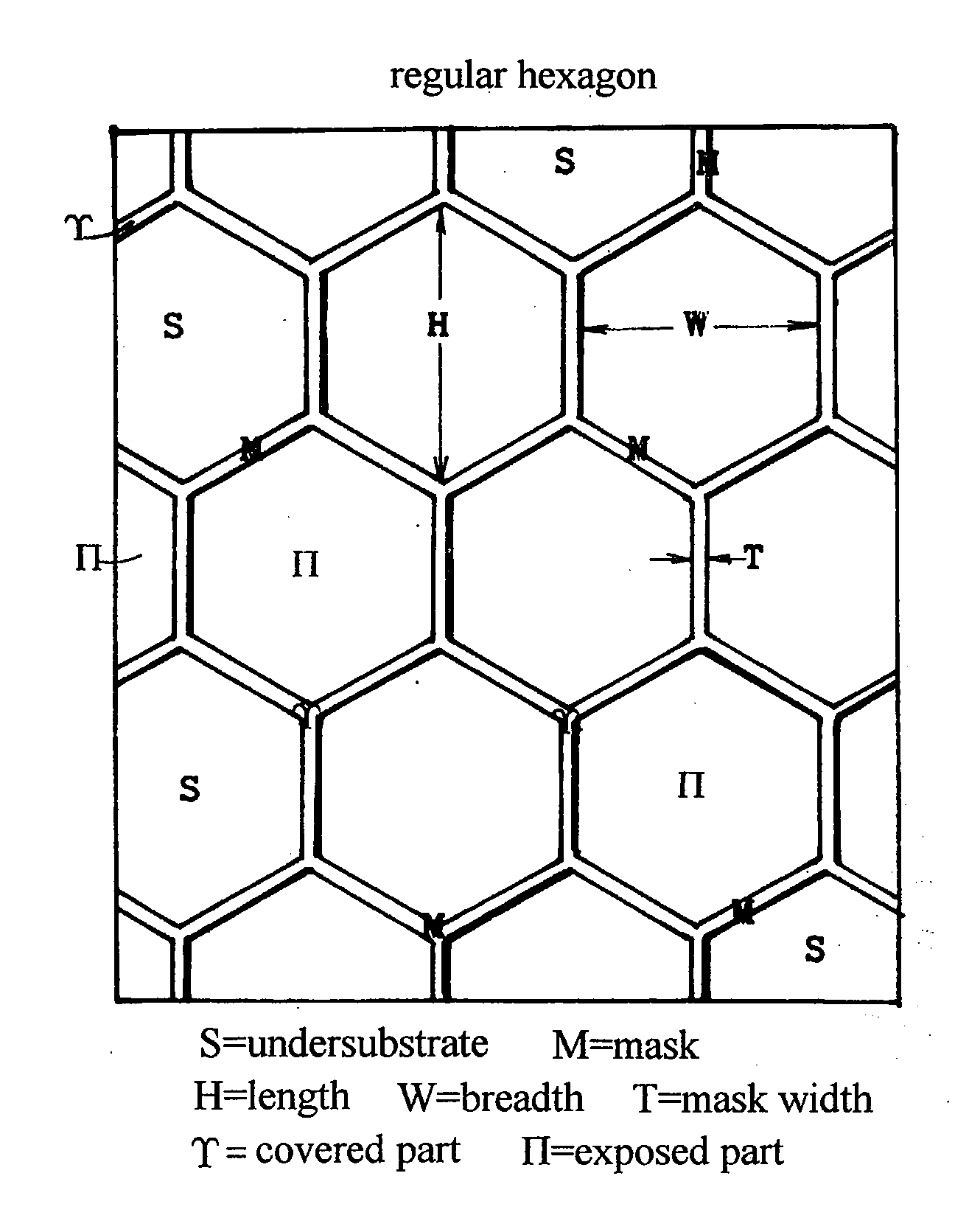
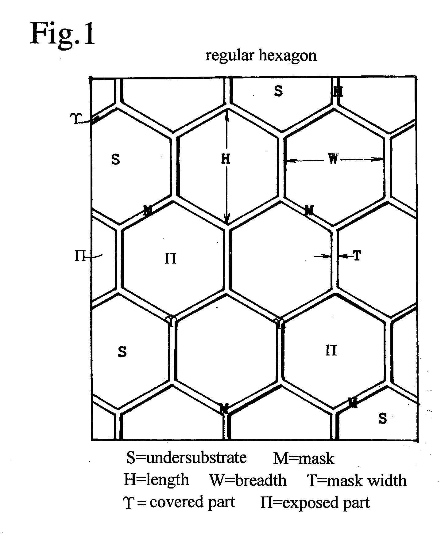
[0165]A sapphire wafer having a thin GaN film of a 2 to 5 μm thickness MOCVD-grown thereupon is prepared as an undersubstrate. This GaN / sapphire wafer is called a sapphire template. Sputtering makes a 100 nm thick SiO2 film on the sapphire template. Conventional photolithography and etching make a SiO2 mask pattern on the sapphire undersubstrate. The layer structure is SiO2 / GaN / Sapphire from top to bottom. FIGS. 11 to 15 demonstrate units of the mask patterns. Although these figures show only one unit pattern, the masks are composed of repetitions of a unit pattern of the same shape and the same size aligning crosswise and lengthwise.
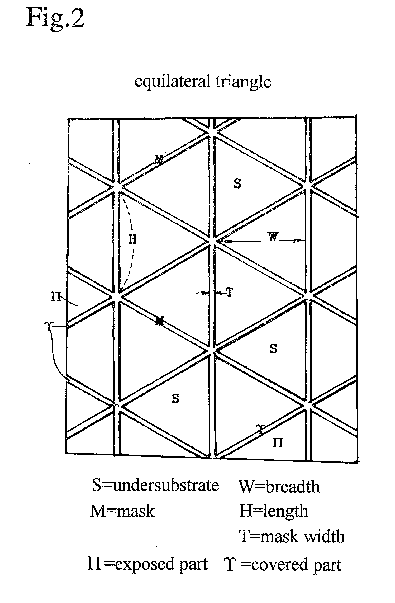
[1. Patterns A-E (Repetitions of Equilateral Triangle Unit Pattern; FIG. 11)]
[0166]FIG. 111 is a unit pattern of an equilateral triangle. The figure shows only a unit pattern. In fact, equivalent equilateral triangle patterns are repeated lengthwise and crosswise. One side of the unit pattern tr...
embodiment 2
GaAs, Si, Sapphire, SiC Undersubstrates; Samples K-N
[0248]Instead of the GaN-templated sapphire undersubstrates employed in Embodiment 1, Embodiment 2 makes use of undersubstrates made of GaAs(111)A (Sample K), Si (Sample L), SiC (Sample M) and sapphire (Sample N). Network masks are made on a variety of undersubstrates. GaN films are grown on the network masked undersubstrates. Properties of the defect accumulating regions H yielded on the masked undersubstrates are examined.
[0249]Here, there are four kinds of SiO2 mask patterns, K, L, M, and N. Every SiO2 mask pattern is produced by piling a SiO2 layer with a thickness of 100 nm on an undersubstrate, and making a pattern by ordinary photolithography and etching. All of the mask patterns are the same regular hexagon.
W (mm)H (mm)T (mm)Pattern K (GaAs undersubstrate)11.20.05Pattern L (Si undersubstrate)11.20.05Pattern M (6h-SiC undersubstrate)11.20.05Pattern N (sapphire undersubstrate)11.20.05
[0250]A GaN film is grown on each undersub...
embodiment 3
SiO2, SiN, Pt, W Mask; Samples O-R
[0283]Keeping the same mask pattern, Samples O—R change materials of masks. SiO2 (Sample O), Si3N4(Sample P), Pt(Sample Q) and W (Sample R) mask are used. All the masks of SiO2, Si3N4, Pt and W have a common 100 nm thickness.
W (mm)H (mm)T (mm)Sample O (SiO2 mask)11.20.05Sample P (Si3N4 mask)11.20.05Sample Q (Pt mask)11.20.05Sample R (W mask)11.20.05
[0284]Thin buffer layers are made at a low temperature on the masked undersubstrates. Thick epitaxial layers are made at a high temperature on the buffer layers.
(A. Formation of a GaN Low Temperature Deposition Layer)
[0285]
Low temperature HVPE method (for buffer layer)Ga-melt temperature:800° C.undersubstrate temperature:490° C.NH3 partial pressure:0.2 atm (20 kPa)HCl partial pressure:2.0 × 10⁻³ atm (200 Pa)Growth time:15 minutesGrowth thickness:50 nm
(B. Formation of a GaN High Temperature Deposition Layer)
[0286]
High temperature HVPE method (for epitaxial layer)Ga-melt temperature:800° C.undersubstrate te...
PUM
| Property | Measurement | Unit |
|---|---|---|
| diameter | aaaaa | aaaaa |
| diameter | aaaaa | aaaaa |
| inner angle | aaaaa | aaaaa |
Abstract
Description
Claims
Application Information