Eureka AIR delivers breakthrough ideas for toughest innovation challenges, trusted by R&D personnel around the world.

Manufacturable reliable diffusion-barrier

Active Publication Date: 2009-07-02
TEXAS INSTR INC
View PDF5 Cites 0 Cited by
  • Summary
  • Abstract
  • Description
  • Claims
  • Application Information

AI Technical Summary

Benefits of technology

[0010]In one exemplary embodiment, the present invention is a method to form an ultra-thin nitride layer on a substrate. This is achieved by initially flowing nitrogen gas in a process chamber, stabilizing the chamber pressure as desired, igniting a DC-target bias component, and stopping the flow of nitrogen into the chamber before the ignition process is complete. The thickness of the nitride layer can thus be controlled by varying the point at which the nitrogen flow is stopped.
[0011]In another exemplary embodiment, the nitrogen gas flow is stopped before the ignition step begins. The pressure of the nitrogen gas is stabilized before the nitrogen flow is stopped. This allows for an even thinner nitride layer.
[0012]In another exemplary embodiment, the present invention is a method to form a metal-barrier layer comprising an ultra-thin nitride layer in combination with a pure metal layer using a single ignition step. A substrate is placed in a PVD chamber along with a metallic target. A combination of gases comprising an inert gas and a reactive gas is introduced into the chamber. A specific ignition voltage is applied to the target to ignite the gas into plasma. Metallic atoms are ejected or “sputtered” from the target towards the substrate. On their way, the metallic atoms react with the nitrogen atoms to form a metallic nitride that is deposited on the substrate forming a nitride barrier layer. While the plasma is being ignited, the nitrogen flow is switched off. Alternatively, the nitrogen flow may be switched off before the plasma is ignited. Thus, the thickness of the nitride layer depends upon the number of nitrogen atoms remaining in the chamber. As the nitrogen atoms in the chamber get depleted, the density of nitride in the layer is reduced, until there are no more nitrogen atoms remaining in the chamber. At this point, metallic atoms continue being deposited on the substrate to form a pure metallic layer. Thus, a metal-barrier layer is formed in one step without having to flush gases in the chamber or reignite plasma.

Problems solved by technology

However the use of copper as an interconnect material present various problems not encountered with the use of aluminum because of the inherent properties of copper and its reaction with silicon and other various dielectrics employed in semiconductor fabrication.
One of the problems is that copper will likely result in diffusion in the silicon or dielectric layer when placed in contact with silicon or dielectric.
This diffusion can lead to the destruction of the underlying circuitry as well as an increase in electromigration.
In addition copper does not bond well with the silicon or most dielectrics.
However, nitride layers do not provide the wettability of a pure metal.
The metal barrier layer, while necessary when using copper, presents problems since it is more resistive than copper and hence leads to slower signal propagation and a slower device.
However, when using sputtering, it is often difficult to consistently produce a layer of either metal or metal nitrate that is less than 2 nm in thickness.
Thus, the typical 2-step sputtering is not a reliable process in manufacturing metal nitrates layers that are loss than 1 nm thick as needed for 65 nm and smaller process used to fabricate semiconductors.
However this process is much more expensive than sputtering.
In addition, the use of ALD to produce a barrier layer has not been proven in terms of reliability.

Method used


Image

  • Manufacturable reliable diffusion-barrier
  • Manufacturable reliable diffusion-barrier
  • Manufacturable reliable diffusion-barrier

Examples


Embodiment Construction

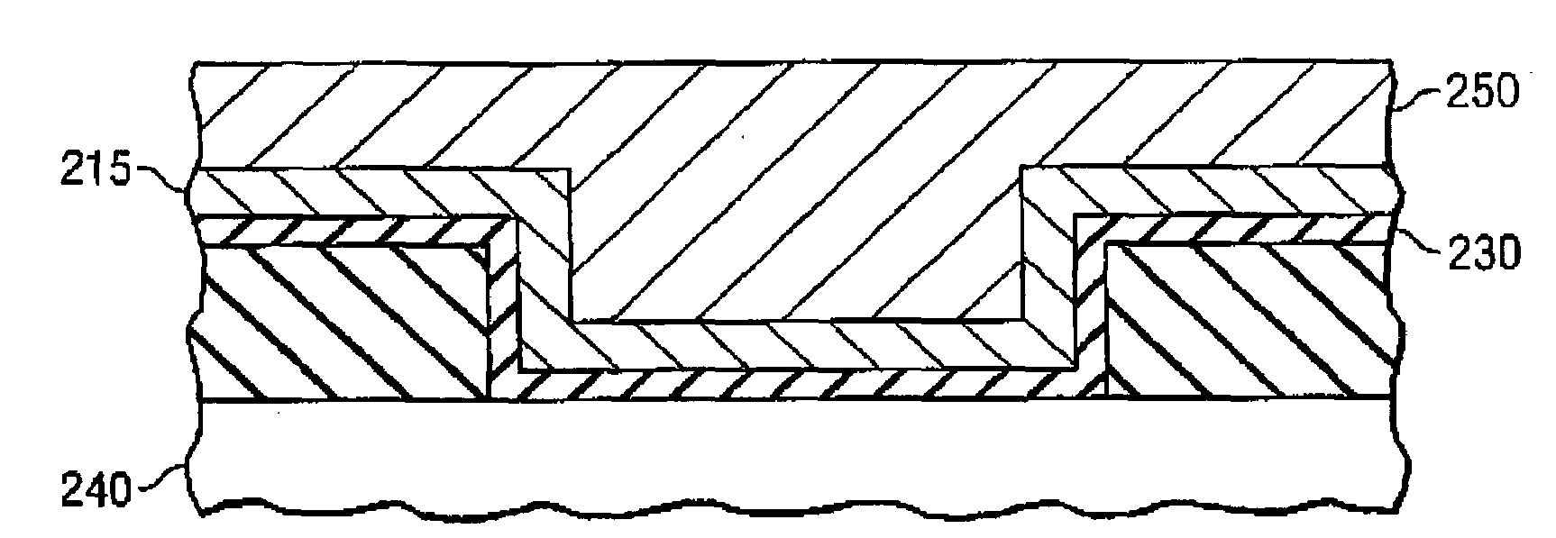
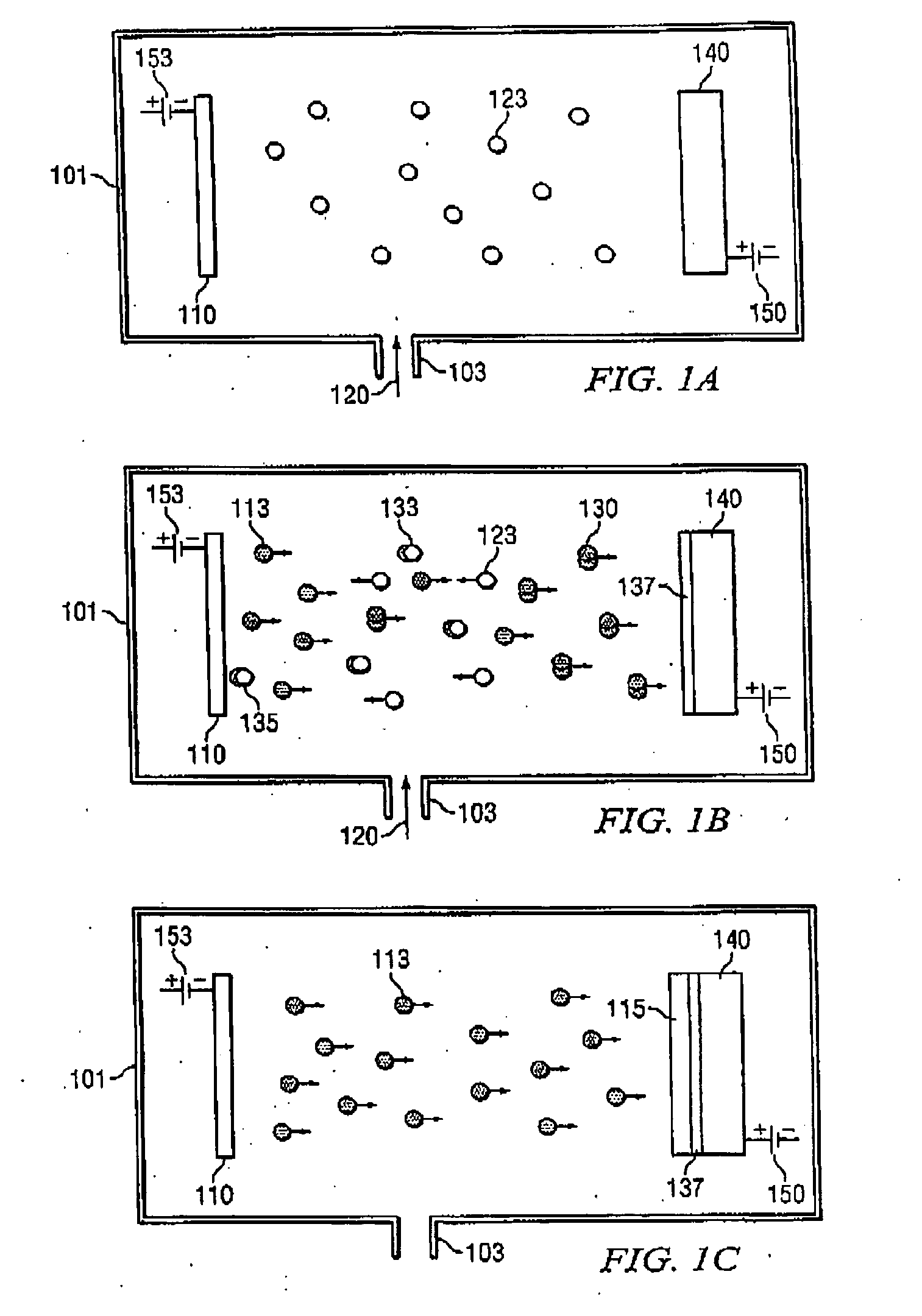
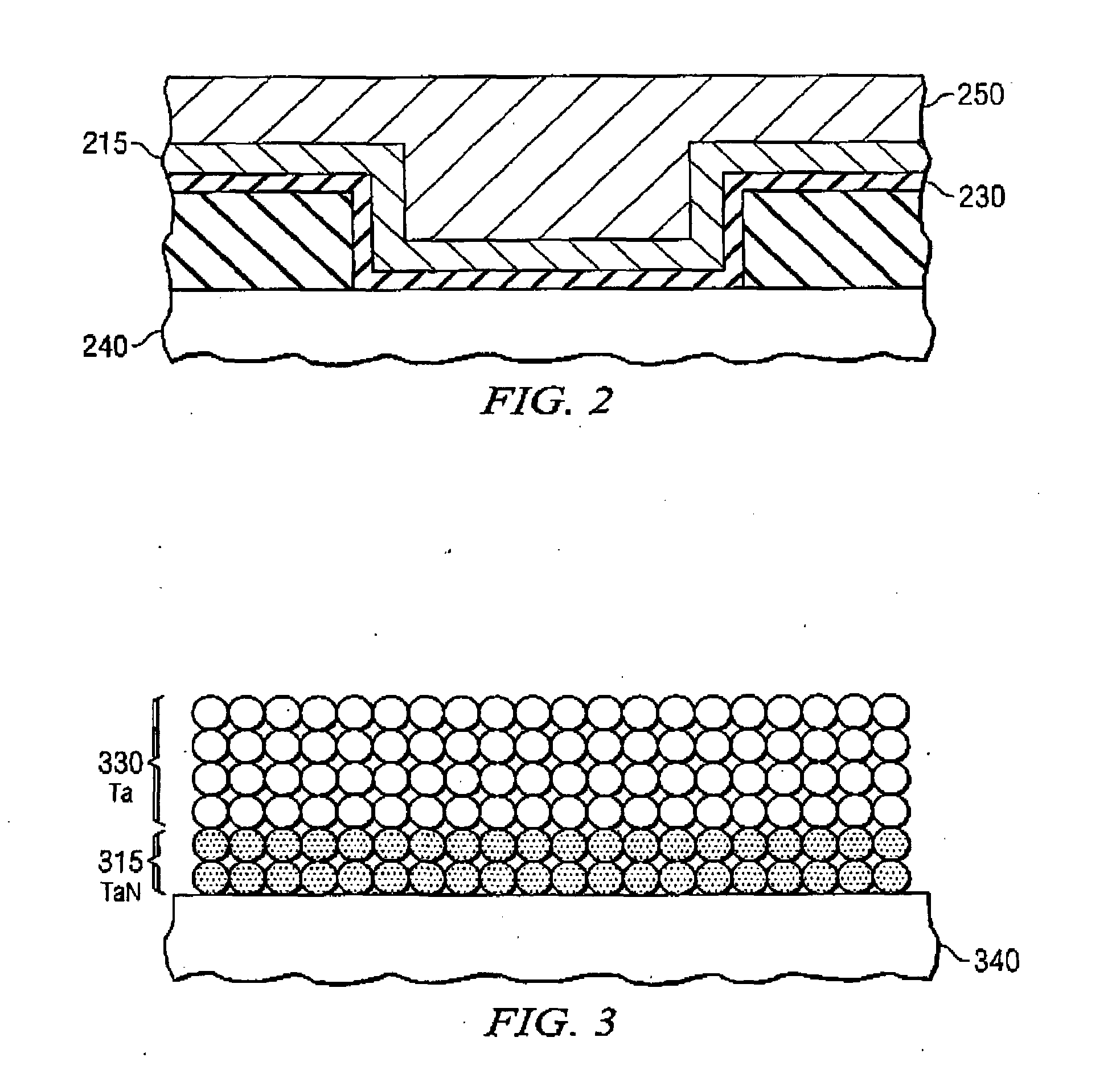
[0016]The present invention discloses methods and devices to make a reliable diffusion barrier less than 1 nm thick that is produced using PVD sputtering. A wafer or a substrate is subjected to a deposition of metal nitride and a pure metal. A gas mixture comprising a reactive gas and a noble gas flows through the chamber at low pressure. An ignition phase starts the flow of plasma that disjoins metallic atoms from a target element. According to the present invention, the flow of reactive gas is stopped either before or during the ignition phase of the sputtering. Thus the flow of the reactive gas is completely stopped before the ignition phase of the sputtering is completed. This ensures that the nitride content of the deposited layer decreases as the layer is deposited on the surface of the substrate. Thus, a very thin layer of metal nitride is formed, wherein the nitride content reduces sharply as distance from the surface increases. Other benefits include improved process contro...


PUM

PropertyMeasurementUnit
Thicknessaaaaaaaaaa
Thicknessaaaaaaaaaa
Flow rateaaaaaaaaaa

Abstract

Devices and methods are presented to fabricate diffusion barrier layers on a substrate. Presently, barrier layers comprising a nitride layer and a pure metal layer are formed using a physical vapor deposition (PVD) process that requires multiple ignition steps, and results in nitride-layer thicknesses of no less than 2 nm. This invention discloses devices and process to produce nitride-layers of less than <1 nm, while allowing for formation of a pure metal layer on the nitride-layer without re-igniting the plasma. To achieve this, the flow of nitrogen gas is cut off either before the plasma is ignited, or before the formation of a continuous-flow plasma. This ensures that a limited number of nitrogen atoms is deposited in conjunction with metal atoms on the substrate, thereby allowing for controlled thickness of the nitride layer.

Description

BACKGROUND OF THE INVENTION[0001]1. Field of the Invention[0002]The present invention relates generally to semiconductor fabrication. More particularly, the present invention relates to the creation of a diffusion barrier layer on a substrate using physical vapor deposition (PVD).[0003]2. Background of the Invention[0004]As microelectronics continue to miniaturize, interconnection performance, reliability, and power consumption have become increasingly important. Interest has grown in replacing aluminum alloys with lower resistivity and higher reliability metals. Copper offers a significant improvement over aluminum as a contact and interconnect material. For example, the resistivity of copper is about half of the resistivity of aluminum. However the use of copper as an interconnect material present various problems not encountered with the use of aluminum because of the inherent properties of copper and its reaction with silicon and other various dielectrics employed in semiconduct...

Claims


Application Information

Patent Timeline
IPC IPC(8): H01L23/48C23C14/00H01L21/44
CPCC23C14/0073C23C14/0641H01L23/53238H01L21/76843H01L21/2855H01L2924/0002H01L2924/00
Inventor RUSSELL, NOEL M.PAPA RAO, SATYAVOLU SRINIVASGRUNOW, STEPHAN
Owner TEXAS INSTR INC
Why Eureka
Eureka Blog
Learn More