Semiconductor light-emitting device, method of manufacturing the same, and lamp including the same

a technology of semiconductor light-emitting devices and semiconductors, which is applied in the direction of semiconductor devices, semiconductor/solid-state device details, electrical apparatus, etc., can solve the problems of difficult to achieve good ohmic contact and strong bonding strength, difficult to sufficiently reduce the contact resistance of an interface, and the effect of reducing the resistance of the sh

Active Publication Date: 2009-07-09
TOYODA GOSEI CO LTD
View PDF8 Cites 25 Cited by
  • Summary
  • Abstract
  • Description
  • Claims
  • Application Information

AI Technical Summary

Benefits of technology

[0033]According to a method of manufacturing a semiconductor light-emitting device of the present invention, an annealing process is performed on a transparent positive electrode, which is laminated on a p-type semiconductor layer and is formed of a transparent conductive oxide material having an oxygen concentration that is lower than a stoichiometric composition, in an atmosphere including oxygen, and a reannealing process is performed on the transparent positive electrode in an oxygen-free atmosphere, thereby obtaining the transparent positive electrode having high translucency, low sheet resistance, a low standard forward voltage Vf, and strong bonding strength to the p-type semiconductor layer. Therefore, a semiconductor light-emitting device fabricated by the manufacturing method according to the present invention can improve brightness, reduce the standard forward voltage Vf, and increase the bonding strength of the transparent positive electrode.
[0034]Further, according to a semiconductor light-emitting device of the present invention, a p-type semiconductor layer side is a light observer side, a transparent positive electrode formed on the p-type semiconductor layer is made of a transparent conductive oxide material, the transparent positive electrode is formed on substantially the entire upper surface of the p-type semiconductor layer, and a bonding pad is formed only on a portion of the transparent positive electrode. In this way, a current can uniformly flow from the transparent positive electrode having low sheet resistance to substantially the entire surface of the p-type semiconductor layer, and it is possible to emit a sufficient amount of light to the outside using the transmittance of the transparent positive electrode. In addition, it is possible to increase the bonding strength between the transparent positive electrode and the p-type semiconductor layer to be stronger than the bonding strength between the bonding pad and the p-type semiconductor layer. Therefore, it is possible to prevent the bonding pad from being peeled off during wire bonding, and thus minimize the possibility of the bonding pad being peeled off during mass production. As a result, it is possible to manufacture a semiconductor light-emitting device having high reliability.

Problems solved by technology

However, when a transparent electrode formed of a transparent conductive oxide material, such as ITO, is formed on a p-type gallium nitride compound semiconductor layer and a bonding pad for connection to an external electric apparatus is formed on the transparent electrode, it is difficult to obtain a good ohmic contact and strong bonding strength between the transparent electrode and the p-type semiconductor layer, and it is difficult to sufficiently reduce the contact resistance of an interface.
In addition, the transparent electrode is likely to be peeled off from the p-type semiconductor layer during wire bonding due to a load applied to the bonding pad.

Method used


Image

  • Semiconductor light-emitting device, method of manufacturing the same, and lamp including the same
  • Semiconductor light-emitting device, method of manufacturing the same, and lamp including the same
  • Semiconductor light-emitting device, method of manufacturing the same, and lamp including the same

Examples


examples

[0095]Next, the present invention will be described in more detail with reference to Examples, but the present invention is not limited thereto.

(Manufacture of Gallium Nitride Compound Semiconductor Light-Emitting Device)

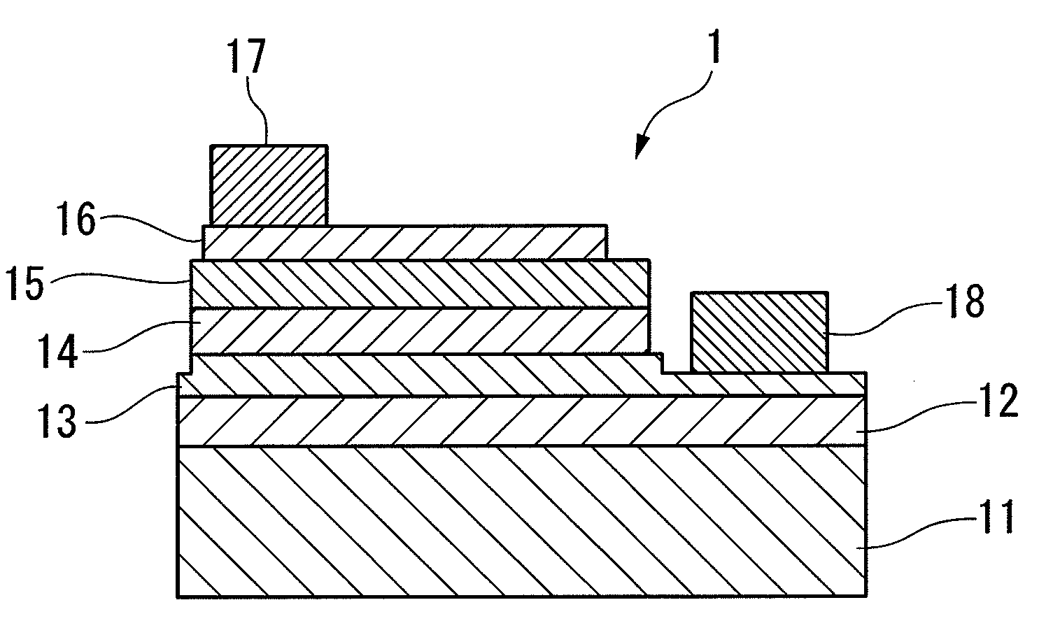
[0096]A gallium nitride compound semiconductor layer was formed on a sapphire substrate 1 with a buffer layer 12 made of AlN interposed therebetween. The gallium nitride compound semiconductor layer was formed by laminating an N-type semiconductor layer 13, a light-emitting layer 14 having a multiple quantum well structure, and a p-type semiconductor layer 15 in this order. The N-type semiconductor layer 13 was formed by laminating an undoped GaN underlying layer with a thickness of 8 μm, a Ge-doped n-type GaN contact layer with a thickness of 2 μm, and an n-type In0.06Ga0.94N clad layer with a thickness of 0.02 μm in this order. The light-emitting layer 14 having a multiple quantum structure was formed by providing a barrier layer on five laminates of a Si-doped Ga...


PUM


Abstract

A semiconductor light-emitting device having a high light emission property and preventing an electrode from being peeled off during wire bonding. Also disclosed is a method of manufacturing a semiconductor light-emitting device 1 in which an n-type semiconductor layer (13), a light-emitting layer (14), and a p-type semiconductor layer (15) are formed on a substrate (11), a transparent positive electrode (16) is formed on the p-type semiconductor layer (15), a positive electrode bonding pad (17) is formed on the transparent positive electrode (16), and a negative electrode bonding pad (18) is formed on the n-type semiconductor layer (13).

Description

TECHNICAL FIELD[0001]The present invention relates to a gallium nitride compound semiconductor light-emitting device and a method of manufacturing the same, and more particularly, to a technique capable of reducing the connection resistance of an electrode.[0002]Priority is claimed on Japanese Patent Application No. 2006-110830, filed Apr. 13, 2006, the content of which is incorporated herein by reference.BACKGROUND ART[0003]As an example of a compound semiconductor light-emitting device, a structure has been proposed in which an n-type gallium nitride compound semiconductor layer and a p-type gallium nitride compound semiconductor layer are formed on a substrate. In recent years, gallium nitride (GaN) compound semiconductor light-emitting devices have drawn attention as short wavelength light-emitting devices. The gallium nitride compound semiconductor light-emitting device is formed by laminating an n-type or p-type semiconductor layer and a light-emitting layer on various kinds o...

Claims


Application Information

Patent Timeline
Patent Type & Authority Applications(United States)
IPC IPC(8): H01L33/00H01L21/28H01L33/62H01L33/06H01L33/32H01L33/38H01L33/42H01L33/56H01L33/60
CPCH01L33/0095H01L33/42H01L2224/32245H01L2224/48091H01L2224/48247H01L2224/48257H01L2224/73265H01L2933/0016H01L2924/3025H01L2924/181H01L2924/00014H01L2924/00H01L2924/00012
Inventor HANAWA, KENZOYOKOYAMA, YASUNORI
Owner TOYODA GOSEI CO LTD
Why Eureka
Try Eureka