Phase-change material, memory unit and method for electrically storing/reading data

a phase-change memory and memory unit technology, applied in the field of phase-change materials and memory units, can solve the problems of difficult control of the characteristics of the above storage unit, low resistance in the memory unit of a phase-change memory (pram), and high loss of current of the unit, so as to avoid incomplete reset

Active Publication Date: 2009-07-23
NAT TAIWAN UNIV
View PDF2 Cites 5 Cited by
  • Summary
  • Abstract
  • Description
  • Claims
  • Application Information

AI Technical Summary

Benefits of technology

[0009]The phase-change material of this invention is in a single crystalline state and has a characteristic of a great discrepancy between high and low resistance states, so that while being used to fabricate the phase-change memory uni

Problems solved by technology

In the past, the resistance in a memory unit of a phase-change memory (PRAM) was relatively low, for instance, just several thousand ohms, and the current of the unit had a high loss owing to the resistance of a transistor.
Therefore, it is difficult to control the characteristics o

Method used


Image

  • Phase-change material, memory unit and method for electrically storing/reading data
  • Phase-change material, memory unit and method for electrically storing/reading data
  • Phase-change material, memory unit and method for electrically storing/reading data

Examples


example 1

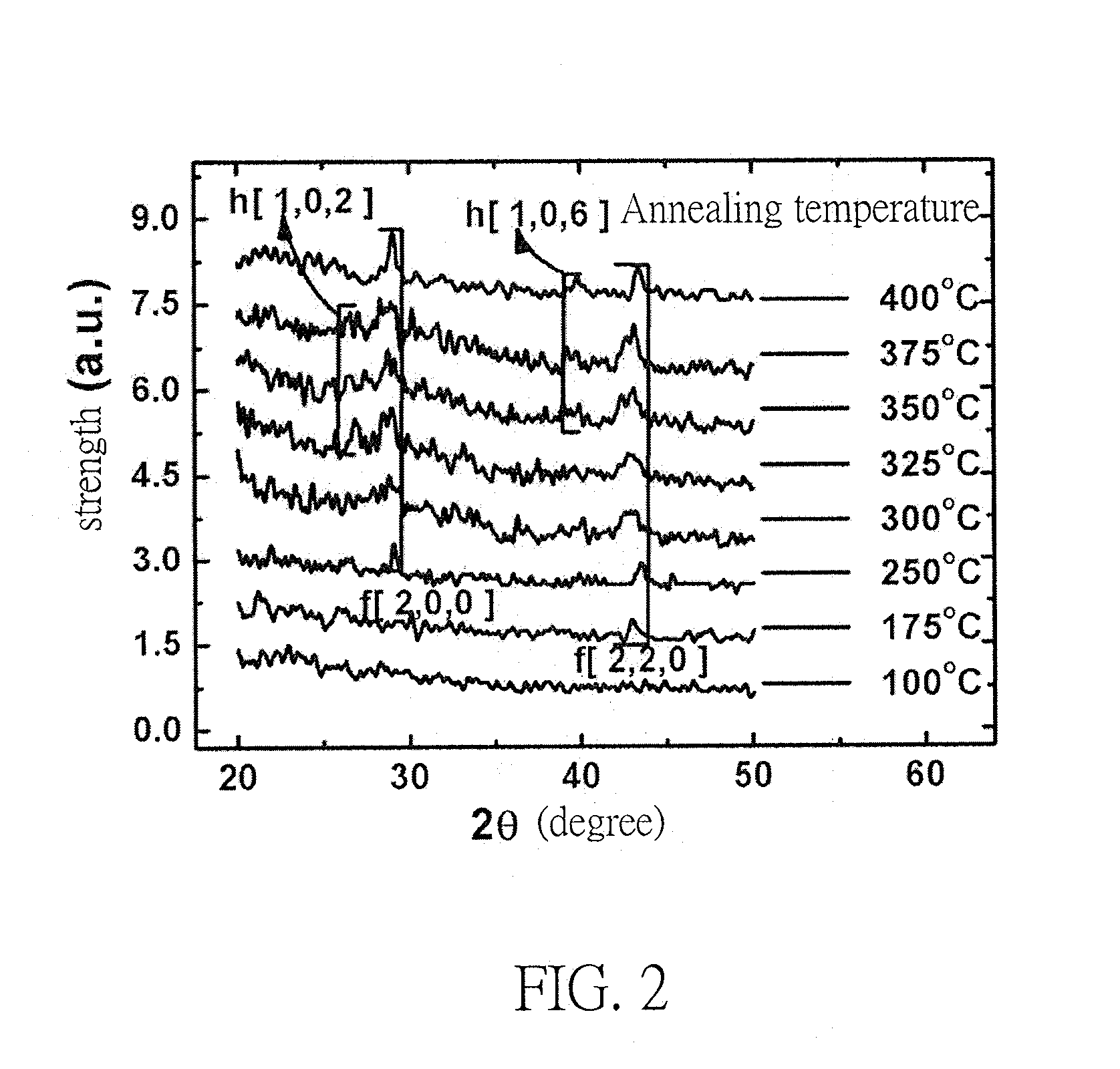
[0041]The phase-change material of InGaON is formed on a silicon wafer by sputter deposition, and then the phase-change thin film of Ge2Sb2Te5 is measured and analyzed by X-ray diffraction. FIG. 3 is an X-ray diffraction pattern showing the temperature effect. While the temperature is higher than 250□, signals of the lattice plane at high peak [222] and short peak [400] appear. The tendency of peak strength increases gradually along with the rising of temperature, and there are more and more crystalline components. After the temperature reaches 500□, the peak strength stops increasing. It is shown in these results that the phase-change material of the present invention has a single crystalline state.

example 2

[0042]A 0.18-micrometer dielectric trench is formed on a metal wire layer of the integrated circuit, and filled with tungsten metal as a bottom substrate. The chamber pressure is controlled by a throttle valve in the vapor deposition process, and the adequate flow amount of oxygen and nitrogen is controlled by MFC. While the chamber pressure is at 8 mtorr, a layer of the phase-change material of Ga—O—N is formed on the bottom substrate and has a thickness of 20 μm. Then, a passivation structure of silicon dioxide and a metal cushion at the top are formed so as to obtain a memory unit sample. A current-voltage graph of the memory unit sample is illustrated in FIG. 4. The resistance at an amorphous state is 2 kΩ, and the resistance at a crystalline state is 160Ω. The critical current for phase change is 43 mA.

example 3

[0043]A layer of the phase-change material of Ge—O—N is formed on the bottom substrate and has a thickness of 20 μm. Then, a passivation structure of silicon dioxide and a metal cushion at the top are formed so as to obtain a memory unit sample. A current-voltage graph of the memory unit sample is illustrated in FIG. 5. The resistance at an amorphous state is 402 kΩ, and the resistance at a crystalline state is 80Ω. The critical current for phase change is about 2 mA.


PUM

PropertyMeasurementUnit
Timeaaaaaaaaaa
Timeaaaaaaaaaa
Thicknessaaaaaaaaaa

Abstract

A phase-change material and a memory unit using the phase-change material are provided. The phase-change material is in a single crystalline state and includes a compound of a metal oxide or nitroxide, wherein the metal is at least one selected from a group consisting of indium, gallium and germanium. The memory unit includes a substrate; at least a first contact electrode formed on the substrate; a dielectric layer disposed on the substrate and formed with an opening for a layer of the phase-change material to be formed therein; and at least a second contact electrode disposed on the dielectric layer. As the phase-change material is in a single crystalline state and of a great discrepancy between high and low resistance states, the memory unit using the phase-changed material can achieve a phase-change characteristic rapidly by pulse voltage and avert any incomplete reset while with a low critical power.

Description

FIELD OF THE INVENTION[0001]The present invention relates to a phase-change material and memory units, and more particularly, to a phase-change material and a memory unit using the same, which are capable of storing / reading data in an electric manner.BACKGROUND OF THE INVENTION[0002]In the field of optical storage, it has been an important and well-developed technology to record digital signals of 0 and 1 generated by the change of refractive index of a phase-change material in different crystalline states, for example, an optical recording layer of an optical disk (CD, DVD). In 1986, investigators of International Business Machines Corporation (IBM) found that a phase-change alloy of germanium-stibium-tellurium (Ge—Sb—Te, GST) converts rapidly in phase by means of the transfer of electrical signals, making this phase-change material be extensively applied to a flash memory that can be operated to transfer electronic signals.[0003]Along with the rapid growth of and increasing demand...

Claims


Application Information

Patent Timeline
IPC IPC(8): G11C11/00H01L45/00C01B21/20C01G15/00C01G17/00
CPCC23C14/0676H01L45/145H01L45/06Y10S438/90H01L45/126H01L45/1625H01L45/1233H10N70/8413H10N70/883H10N70/231H10N70/026H10N70/826
Inventor PENG, LUNG-HANWANG, SUNG-LIHSIEH, MENG-KUEICHEN, CHIEN-YU
Owner NAT TAIWAN UNIV
Why Eureka
Try Eureka