Group-iii nitride compound semiconductor device and production method thereof, group-iii nitride compound semiconductor light-emitting device and production method thereof, and lamp

a technology of compound semiconductors and light-emitting devices, which is applied in the direction of semiconductor lasers, vacuum evaporation coatings, coatings, etc., can solve the problems of reducing the light-emitting efficiency of light-emitting devices, reducing the level of threading dislocation within the base layer, and reducing the emission intensity. , the effect of excellent uniformity

Inactive Publication Date: 2009-08-06
SHOWA DENKO KK
View PDF18 Cites 49 Cited by
  • Summary
  • Abstract
  • Description
  • Claims
  • Application Information

AI Technical Summary

Benefits of technology

[0019]Furthermore, the inventors of the present invention also focused their attention on the mechanism for the generation of threading dislocations. In particular, because the level of threading dislocation within the base layer can be reduced by using an intermediate layer of excellent uniformity, they investigated methods capable of achieving excellent uniformity for the intermediate layer interposed between the substrate and the base layer. As a result, they discovered that an intermediate layer formed using a sputtering method has superior in-plane uniformity to an intermediate layer formed using a MOCVD method, even when the formed film is very thin, and that by using a sputtering method to form the intermediate layer interposed between the substrate and the base layer, the level of threading dislocation within the base layer could be reduced, and they were therefore able to complete the present invention.
[0020]A group-III nitride compound semiconductor light-emitting device of the present invention has a base layer provided on an intermediate layer provided on a substrate, in which a full width at half maximum in rocking curve of a (0002) plane is 100 arcsec or lower and a full width at half maximum in rocking curve of a (10-10) plane is 300 arcsec or lower, and consequently the level of threading dislocation within the semiconductor layer is minimal, and excellent light emission properties can be obtained.
[0021]Further, according to a production method of a group-III nitride compound semiconductor light-emitting device of the present invention, because the intermediate layer is formed using a sputtering method, a uniform intermediate layer can be formed, meaning a base layer in which a full width at half maximum in rocking curve of a (0002) plane is 100 arcsec or lower and a full width at half maximum in rocking curve of a (10-10) plane is 300 arcsec or lower can be formed on the intermediate layer with comparative ease. Accordingly, the production method of a group-III nitride compound semiconductor light-emitting device according to the present invention can readily provide a group-III nitride compound semiconductor light-emitting device of the present invention having minimal threading dislocation within the semiconductor layer and excellent light emission properties.
[0022]Furthermore, in the present invention, by adopting a layer constitution in which the n-type cladding layer and / or the p-type cladding layer includes a superlattice structure, a light-emitting device having markedly improved output and superior electrical properties can be obtained.
[0023]Moreover, a lamp of the present invention uses a group-III nitride compound semiconductor light-emitting device of the present invention, and therefore has excellent light emission properties.

Problems solved by technology

However, when a group-III nitride compound semiconductor is formed on a sapphire substrate, lattice constant misfit between the sapphire and the group-III nitride compound semiconductor causes dislocation, which has an adverse effect on the device properties.
Accordingly, threading dislocation within the semiconductor layer of a light-emitting device causes a reduction in the light emission efficiency of the light-emitting device, resulting in reduced emission intensity.
However, even when a group-III nitride compound semiconductor is grown on a substrate with an intermediated layer disposed therebetween, threading dislocation within the semiconductor layer cannot be prevented entirely satisfactorily, and there is considerable demand for semiconductor layers having an even lower level of threading dislocation.

Method used


Image

  • Group-iii nitride compound semiconductor device and production method thereof, group-iii nitride compound semiconductor light-emitting device and production method thereof, and lamp
  • Group-iii nitride compound semiconductor device and production method thereof, group-iii nitride compound semiconductor light-emitting device and production method thereof, and lamp
  • Group-iii nitride compound semiconductor device and production method thereof, group-iii nitride compound semiconductor light-emitting device and production method thereof, and lamp

Examples


example 1

[0159]A layer formed of AlN was formed as an intermediate layer on the c-plane of a sapphire substrate using a RF sputtering method, and a layer formed of GaN was then formed as a base layer on top of the intermediate layer using a MOCVD method.

[0160]A c-plane sapphire substrate was placed in a sputtering apparatus, the substrate was heated to 500° C. inside the chamber of the apparatus, and nitrogen gas was introduced into the chamber at a flow rate of 15 sccm. Subsequently, with the pressure inside the chamber held at 1 Pa, a 500 W high-frequency bias was applied to the substrate side, and the surface of the substrate was cleaned by exposure to nitrogen plasma.

[0161]Subsequently, argon gas and nitrogen gas were introduced into the chamber, and the substrate temperature was set to 500° C. High-frequency power of 2,000 W was then applied to the target side, and with the pressure inside the chamber held at 0.5 Pa and under conditions including an argon gas flow rate of 5 sccm and a n...

example 2

[0165]In Example 2, with the exception of altering the conditions during cleaning of the substrate surface and the conditions during formation of the intermediate layer, an intermediate layer and a base layer were formed on a substrate in the same manner as Example 1.

[0166]A c-plane sapphire substrate was placed in a sputtering apparatus, the substrate was heated to 750° C. inside the chamber of the apparatus, and nitrogen gas was introduced into the chamber at a flow rate of 15 sccm. Subsequently, with the pressure inside the chamber held at 0.08 Pa, a 500 W high-frequency bias was applied to the substrate side, and the surface of the substrate was cleaned by exposure to a nitrogen plasma.

[0167]Subsequently, argon gas and nitrogen gas were introduced into the chamber, and the substrate temperature was cooled to 500° C. High-frequency power of 2,000 W was then applied to the target side, and with the pressure inside the chamber held at 0.5 Pa and under conditions including an argon ...

example 3

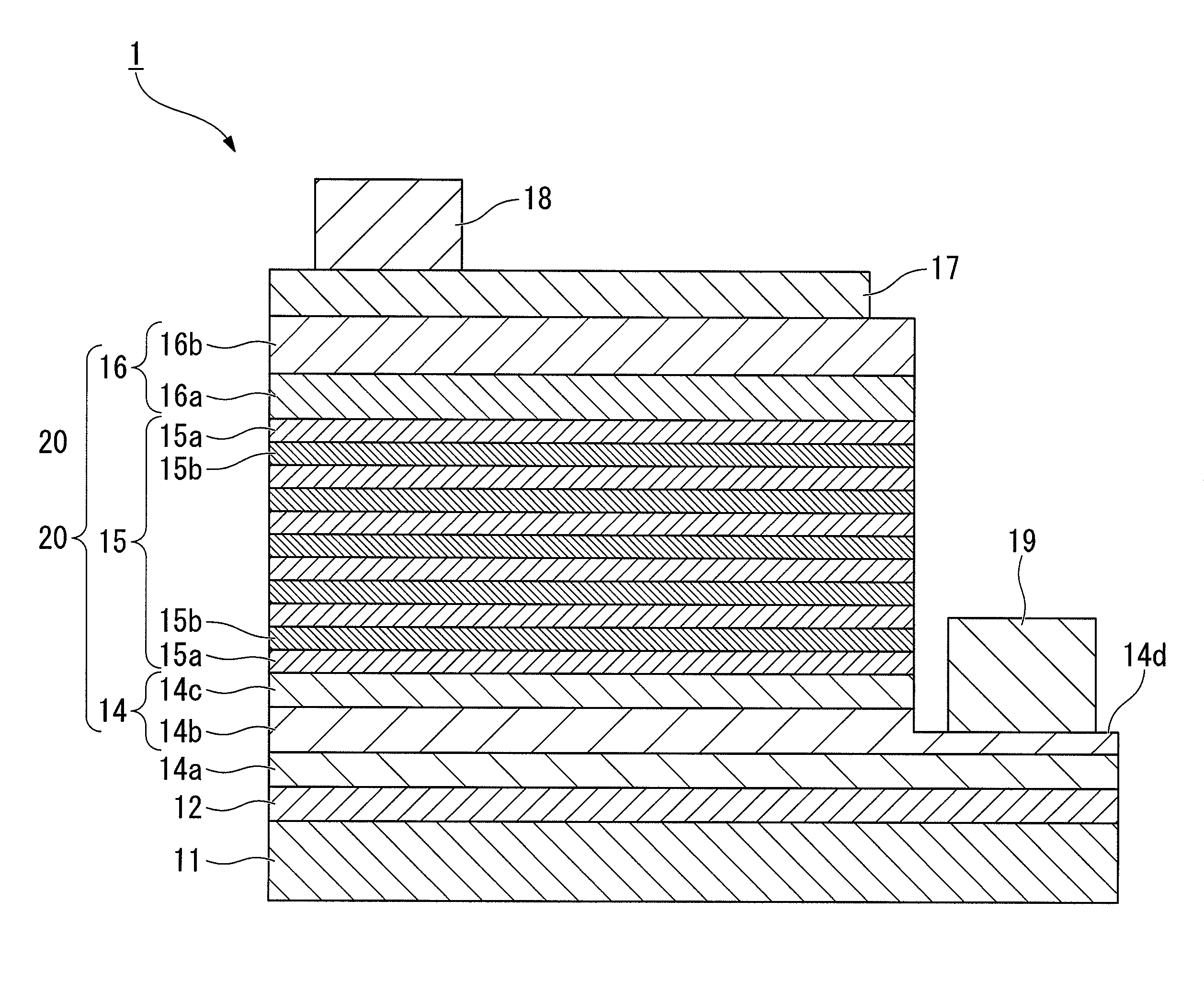
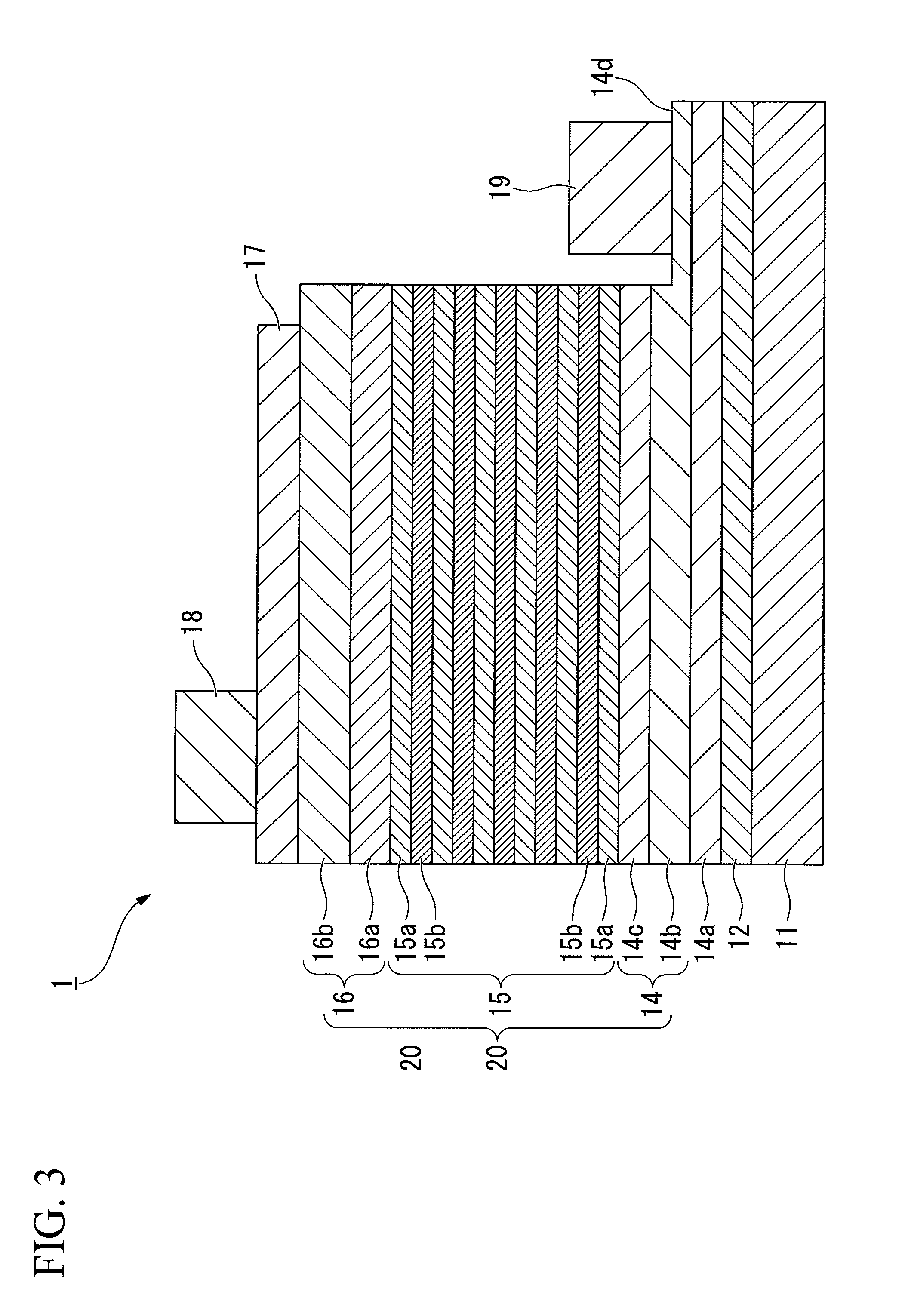
[0179]As Example 3, a light-emitting device 1 similar to that shown in FIG. 3 and FIG. 4 (refer also to the laminated semiconductor 10 of FIG. 5) was prepared, and a lamp 3 (a light-emitting diode: LED) similar to that shown in FIG. 6 that used the light-emitting device 1 was then prepared.

[0180]In this example, first, a RF sputtering method was used to form a single crystal layer formed of AlN as an intermediate layer 12 on the c-plane of a substrate 11 composed of sapphire, and a MOCVD method was then used to form a layer formed of GaN (a group-III nitride compound semiconductor) as a base layer 14a on top of the intermediate layer 12. Each of the other layers was then laminated onto the substrate.

[0181]First, a substrate 11 formed of a 2-inch diameter (0001) c-plane sapphire that had been polished to a mirror surface was placed inside a chamber. A high-frequency sputtering apparatus was used, and a target formed of metallic Al was used as the target.

[0182]The substrate 11 was hea...


PUM

PropertyMeasurementUnit
full width at half maximumaaaaaaaaaa
semiconductoraaaaaaaaaa
emission spectrumaaaaaaaaaa

Abstract

A group-III nitride compound semiconductor device of the present invention comprises a substrate, an intermediate layer provided on the substrate, and a base layer provided on the intermediate layer in which a full width at half maximum in rocking curve of a (0002) plane is 100 arcsec or lower and a full width at half maximum in rocking curve of a (10-10) plane is 300 arcsec or lower. Also, a production method of a group-III nitride compound semiconductor device of the present invention comprises forming the intermediate layer by using a sputtering method.

Description

TECHNICAL FIELD[0001]The present invention relates to a group-III nitride compound semiconductor device that can be used favorably in a light-emitting diode (LED), a laser diode (LD) or an electronic device or the like, and a production method of such a semiconductor device, a group-III nitride compound semiconductor light-emitting device and a production method thereof, and a lamp that uses a group-III nitride compound semiconductor light-emitting device.[0002]Priority is claimed on Japanese Patent Application No. 2007-6790, filed Jan. 16, 2007, Japanese Patent Application No. 2007-184456, filed Jul. 13, 2007, Japanese Patent Application No. 2007-274458, filed Oct. 22, 2007, and Japanese Patent Application No. 2007-286691, filed Nov. 2, 2007, the contents of which are incorporated herein by reference.BACKGROUND ART[0003]A group-III nitride compound semiconductor is a direct transition-type semiconductor which, for example, when used as a light-emitting device, has an emission spect...

Claims


Application Information

Patent Timeline
Patent Type & Authority Applications(United States)
IPC IPC(8): H01L33/00H01L29/205H01L29/20H01L21/20H01L33/16H01L33/06H01L33/12H01L33/32H01L33/42H01L33/56H01L33/62
CPCH01L21/0242H01L21/02433H01L2224/73265H01L2224/49107H01L2224/48257H01L2224/48247H01L2224/48091H01L2224/32245H01L2224/45144H01L33/34H01L33/16H01L21/0262H01L21/0254H01L21/02458H01L2924/00014H01L2924/00B82Y20/00C23C14/0641C23C16/34H01L21/0237H01L21/02631H01L33/007H01L33/12H01S5/34333H01L2924/181C23C14/0617C23C16/303H01L21/02576H01L21/02579H01S5/0213H01S5/32025H01L2924/00012
Inventor KAJI, HIROAKIYOKOYAMA, YASUNORISAKAI, HIROMITSU
Owner SHOWA DENKO KK
Why Eureka
Try Eureka