Method of making diamond nanopillars

a diamond nanoparticle and nanoparticle technology, applied in the direction of crystal growth process, polycrystalline material growth, chemically reactive gas, etc., can solve the problem of difficult structure to a desired geometry to fully explore the advantages of diamond in different applications, and achieve the effect of expanding the application potential of diamond

Active Publication Date: 2009-09-17
CITY UNIVERSITY OF HONG KONG
View PDF6 Cites 55 Cited by
  • Summary
  • Abstract
  • Description
  • Claims
  • Application Information

AI Technical Summary

Benefits of technology

[0008]The formation of high density diamond nanopillars can extend the application potential of diamond, particularly in the biomedical and electrochemical fields. Accordingly, it is an objection of the present invention to provide a method for fabric

Problems solved by technology

However, the extreme properties of diamond make it difficult to structure to

Method used


Image

  • Method of making diamond nanopillars
  • Method of making diamond nanopillars
  • Method of making diamond nanopillars

Examples


example 1

[0033]Nano-D films were deposited using a commercial ASTeX microwave plasma CVD (MWCVD) reactor equipped with a 5 kW microwave generator as shown in FIG. 1. N-type (001) silicon wafers of 3 inches in diameter were used as substrates. Prior to deposition, the substrate was ultrasonically abraded for 60 min in a suspension of nano-D powders with the grain size of ˜5 nm in ethanol. A 10% CH4 / H2 gas mixture was used as the reactive gas source for nano-D deposition. The total gas flow rate was 200 sccm and the pressure was maintained at 30 torr. The microwave power and deposition temperature were set at 1200 W and 800 degrees-C., respectively. The gold films employed as etching masks were deposited onto the deposited nano-D film with a magnetron sputtering system (Auto 306, Edwards). The thickness of the gold layer mask was about 5 nm.

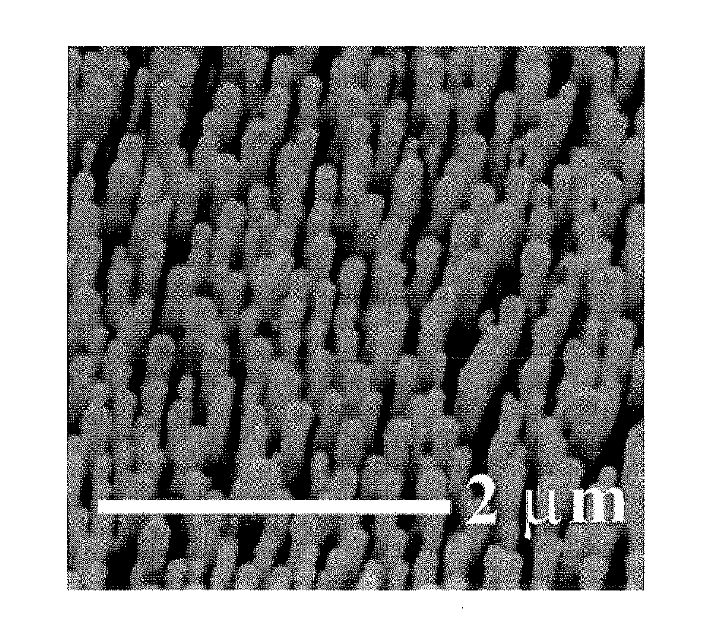
[0034]FIG. 2 shows the SEM plain-view image of a nano-D film pre-coated with a thin gold mask layer. The sample was used as the starting material for struc...

example 2

[0038]Micro-D films can also be structured into diamond nanopillar arrays. The micro-D deposition and structuring were performed in the same deposition system as described above in example 1. The bias-enhanced nucleation (BEN) was used to enhance nucleation for the micro-D deposition, and the BEN was performed in a 5% CH4 / 95% H2 gas mixture at dynamic pressure of 20 Torr provided with a total gas flow rate of 300 sccm. The plasma was induced with a microwave power of 800 W. The substrate temperature was 850 degrees-C. and substrate bias was maintained at −150 V. The BEN took 15 minutes. During the process of diamond growth, the methane concentration was reduced to 0.5%, the total gas flow was kept at 300 sccm, and the total pressure was adjusted to 30 torr. The substrate was maintained 800 degrees-C., while the microwave power was increased to 1200 W.

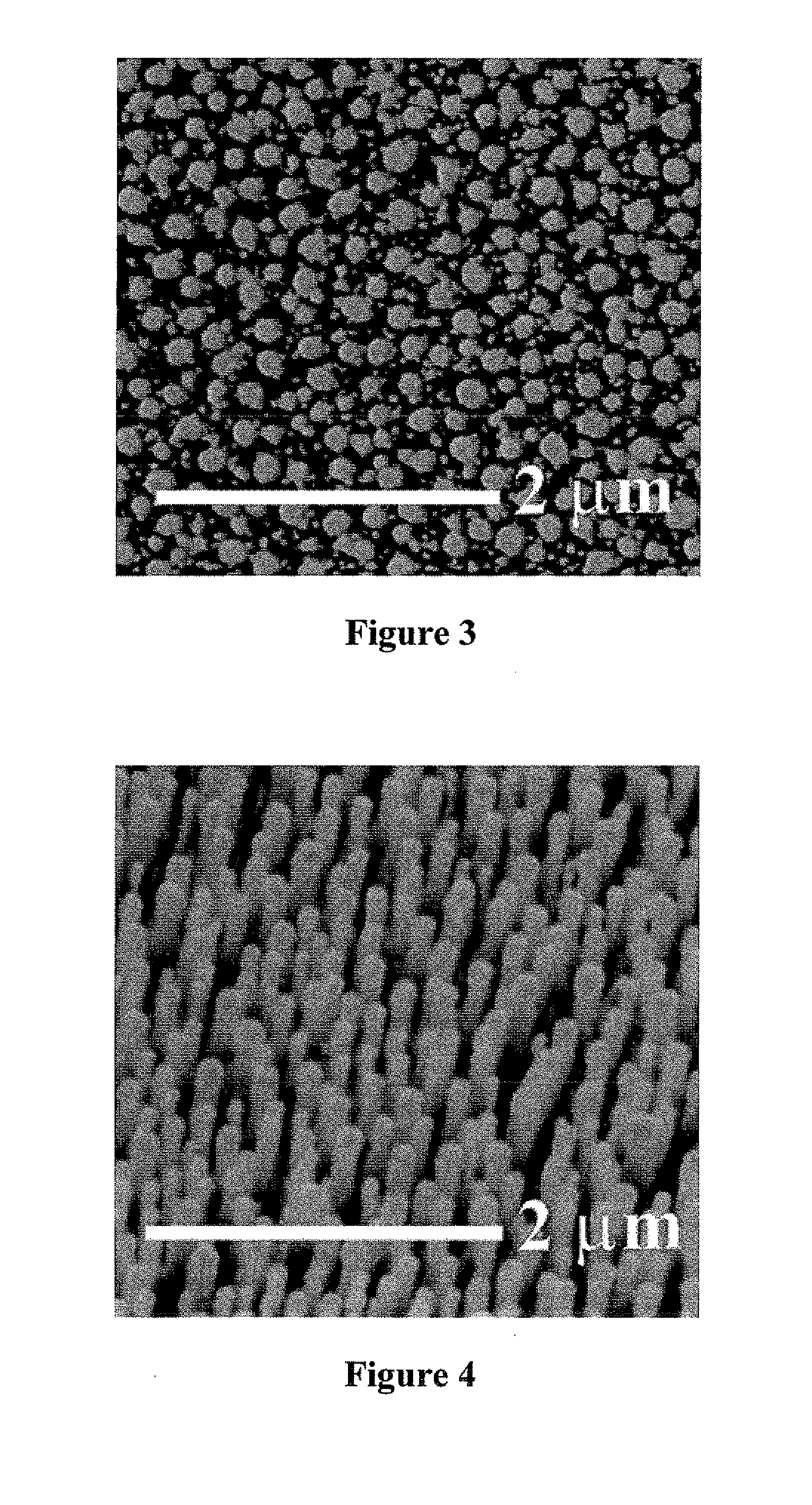
[0039]FIG. 6 shows the SEM plain-view image of a randomly-oriented micro-D film deposited on silicon substrate. The diamond film is ab...


PUM


Abstract

A method for fabricating diamond nanopillars includes forming a diamond film on a substrate, depositing a metal mask layer on the diamond film, and etching the diamond film coated with the metal mask layer to form diamond nanopillars below the mask layer. The method may also comprise forming diamond nuclei on the substrate prior to forming the diamond film. Typically, a semiconductor substrate, an insulating substrate, a metal substrate, or an alloy substrate is used.

Description

BACKGROUND TO THE INVENTION[0001]1. Field of the Invention[0002]This invention relates to the fabrication of diamond nanopillars. The invention also relates to diamond nanopillar arrays.[0003]2. Background Information[0004]Due to its unique combination of outstanding physical and chemical properties, such as wide band-gap, chemical inertness, the highest hardness and thermal conductivity, negative electron affinity, and biocompatibility, diamond is considered to be a promising material for application in electronic and micro-electromechanical devices, biomedical sensors and electrochemical electrodes, and field electron emission (FEE) devices. Diamond can be synthesized in bulk crystalline forms using a high-pressure and high-temperature method and in film forms employing chemical vapor deposition (CVD), typically in a hydrogen environment (including plasma) with a carbon precursor. Highly-oriented diamond films have been available and prepared on various substrates using bias-enhan...

Claims


Application Information

Patent Timeline
IPC IPC(8): H01L21/311C23F1/02
CPCB82Y15/00B82Y30/00C23C16/27C23C16/56Y10S438/947C30B29/04C30B29/60B29C59/14C30B25/105
Inventor LEE, SHUIT-TONGZHANG, WENJUNBELLO, IGORZOU, YOU-SHENG
Owner CITY UNIVERSITY OF HONG KONG
Why Eureka
Try Eureka