Semiconductor light-emitting element and process for production thereof

Inactive Publication Date: 2009-10-01
KK TOSHIBA
View PDF7 Cites 39 Cited by
  • Summary
  • Abstract
  • Description
  • Claims
  • Application Information

AI Technical Summary

Benefits of technology

[0045]In the present invention, the radius of gyration of the opening is defined as follows. On an image of the opening, circular lines at equal intervals are drawn from the edge. In concrete, on a relief image obtained by an atomic force microscopy, circular lines at equal intervals are drawn from the edge. The thus-obtained lines are image-processed to obtain the center of gravity. The distance from the center of gravity to the concavity is then determined, and is processed together with the moment to calculate the radius of gyration R. The radius of gyration can be also obtained by Fourier transform of the electron or atomic force micrograph.
[0046]The larger the surface structure is, the more light is scattered. The effect of light-scattering is in proportion to the square of the size. Accordingly, the average radius of gyration R of the openings is preferably not more than ⅙ of the wavelength of incident light. That is to say, the average diameter of the openings is preferably not more than ⅓ of the wavelength of incident light. If the average radius of gyration R is larger than that, Rayleigh scattering is liable to occur and the light is immediately diffused. The diameter of the openings is more preferably not more than ⅕, further preferably not more than 1/10 of the wavelength of light. As long as the above conditions are satisfied, the shapes of the openings are not particularly restricted. Examples of the opening shapes include cylindrical shape, conical shape, triangular pyramidal shape, quadrilateral pyramidal shape, and other columnar or pyramidal shapes. Two or more shapes may be mixed. Even if the light-transmitting metal electrode according to the present invention contains various sizes of openings, the effect of the invention can be obtained. It is, on the contrary, rather preferred that the openings have various sizes because the metal part with those openings is apt to continue linearly in a relatively lon

Problems solved by technology

Further, because of low contact resistance, the resultant device can work stably.
However, in the case where a metal electrode is adopted, a light-emitting area is small because the electric current flows only just under the electrode or near there.
Further, it is also a problem that light emitted from the active layer is shaded by the opaque metal electrode.
As a resul

Method used


Image

  • Semiconductor light-emitting element and process for production thereof
  • Semiconductor light-emitting element and process for production thereof
  • Semiconductor light-emitting element and process for production thereof

Examples


Example

Example 1

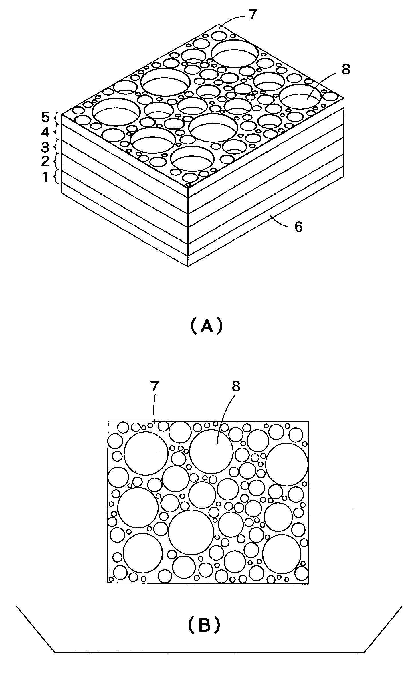
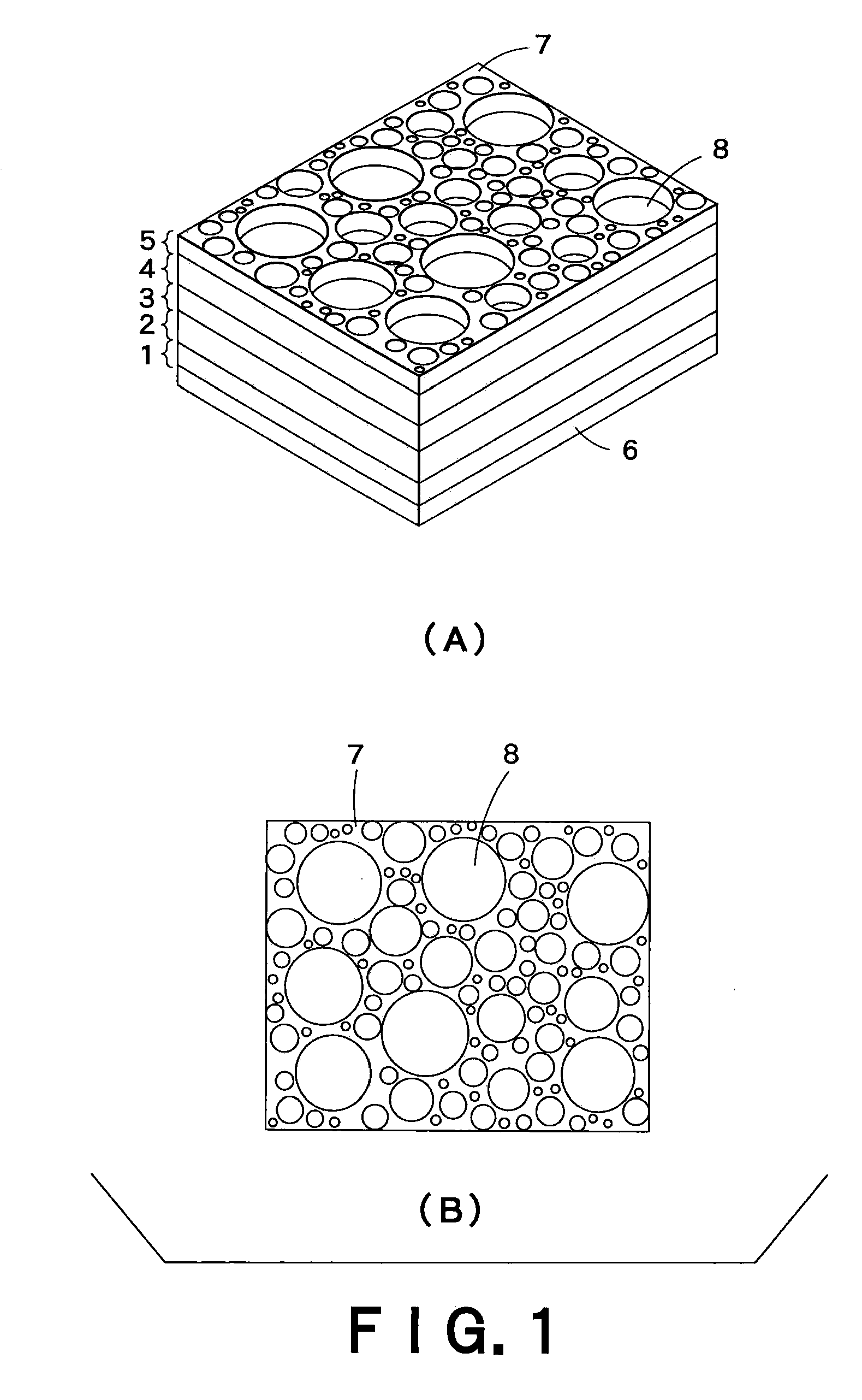
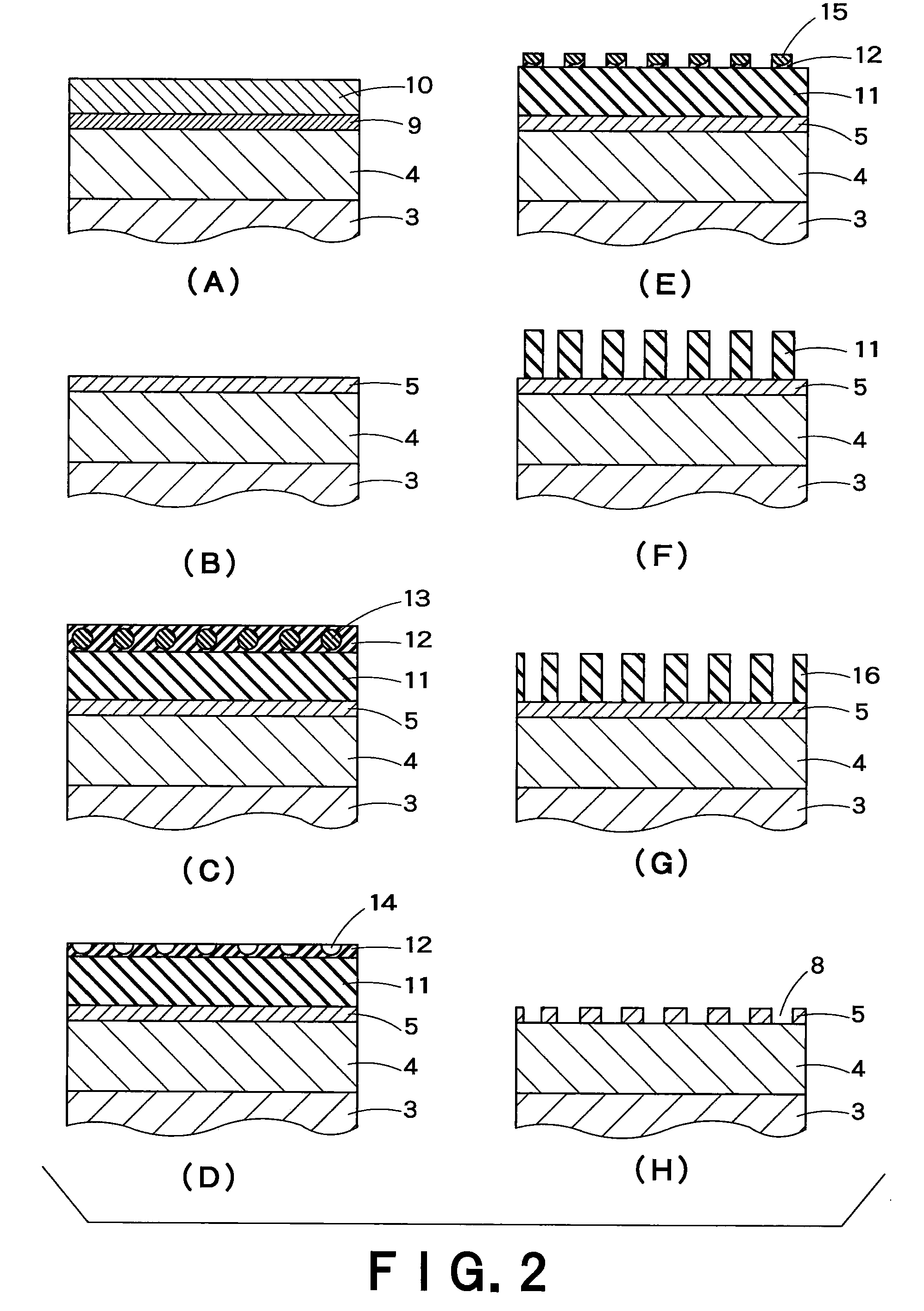
[0071]Firstly, a semiconductor light-emitting element comprising an active layer of InGaAIP in DH structure was produced.

[0072]The (100) face of n-type Si-doped GaAs was used as a crystal substrate. On the substrate, an n-type semiconductor layer (thickness: 1 ρm) made of n-In0.5(Ga0.3Al0.7)0.5P doped with Si was formed by the MOCVD method from trimethylindium (hereinafter, referred to as “TMI”), trimethylgallium (hereinafter, referred to as “TMG”), trimethylaluminum (hereinafter, referred to as “TMA”), PH3 and SiH4. Successively, an active layer of In0.5(Ga0.8Al0.2)0.5P having 0.6 μm thickness was formed thereon from TMI, TMG, TMA and PH3, and then a p-type semiconductor layer (thickness: 1 μm) of p-In0.5(Ga0.3Al0.7)0.5P doped with Zn was produced from TMI, TMG, TMA, PH3 and dimethylzinc (hereinafter, referred to as “DMZ”). Further, a current-spreading layer (thickness: 5 ρm) of p-GaP doped with Zn was formed from TMG, PH3 and DMZ.

[0073]Thereafter, on the whole bottom surf...

Example

Comparative Example 1

[0085]A semiconductor light-emitting element having the same structure as that in Example 1, except that the p-type electrode layer consists of only a pad electrode of Au / AuZn, was produced as a comparative light-emitting element. The pad electrode was produced in the following manner. First, a photosensitive resist was coated on the current-spreading layer of p-GaP, exposed to light by exposure apparatus, and developed to form a resist mask having openings of 100 μm diameter. On the resist mask, an Au thin film and an AuZn alloy thin film were deposited by the vapor-deposition process to form a layered film of 50 nm thickness. Thereafter, the resist part was removed by oxygen plasma RIE to form a pad electrode having openings of 100 μm diameter. The sample was then subjected to heat treatment under nitrogen gas atmosphere to form an ohmic contact between the current-spreading layer and the electrode, and then cut into a chip of 350 μm square to produce a compar...

Example

Example 2

[0087]Secondly, a semiconductor light-emitting element comprising an active layer of InGaAIP in DH structure and an n-type semiconductor layer on the light-extraction side was produced.

[0088]On a p-GaAs substrate, a p-type semiconductor layer (thickness: 1 μm) of p-In0.5(Ga0.3Al0.7)0.5P doped with Zn was formed by the MOCVD method. Successively, an active layer of In0.5(Ga0.8Al0.2)0.5P having 0.6 μm thickness was formed, and then an n-type semiconductor layer (thickness: 1 μm) of n-In0.5(Ga0.3Al0.7)0.5P doped with Si was formed thereon. Further, a current-spreading layer (thickness: 5 μm) of n-GaP doped was formed thereon.

[0089]Thereafter, on the whole bottom surface of the p-GaAs substrate, an Au thin film (thickness: 50 nm) was vapor-deposited and then an AuZn-alloy thin film (thickness: 200 nm) was deposited thereon to form a p-type electrode layer. On the other hand, on the current-spreading layer, another Au thin film (thickness: 50 nm) and an AuGe-alloy thin film (thi...


PUM


Abstract

The present invention provides a semiconductor light-emitting element comprising an electrode part excellent in ohmic contact and capable of emitting light from the whole surface. An electrode layer placed on the light-extraction side comprises a metal part and plural openings. The metal part is so continuous that any pair of point-positions in the part is continuously connected without breaks, and the metal part in 95% or more of the whole area continues linearly without breaks by the openings in a straight distance of not more than ⅓ of the wavelength of light emitted from an active layer. The average opening diameter is of 10 nm to ⅓ of the wavelength of emitted light. The electrode layer has a thickness of 10 nm to 200 nm, and is in good ohmic contact with a semiconductor layer.

Description

CROSS-REFERENCE TO RELATED APPLICATIONS[0001]This application is based upon and claims the benefit of priority from the prior Japanese Patent Applications No. 77421 / 2008, filed on Mar. 25, 2008; the entire contents of which are incorporated herein by reference.BACKGROUND OF THE INVENTION[0002]1. Field of the Invention[0003]The present invention relates to a semiconductor light-emitting element comprising a light-transmitting metal electrode provided with fine openings, and also relates to a process for production thereof.[0004]2. Background Art[0005]A metal electrode is generally employed as an electrode provided on a semiconductor layer in a semiconductor light-emitting element. If produced from metals by the alloying process, the electrode is brought into such good ohmic contact with the semiconductor layer that a great deal of electric current can be injected into an active layer. Further, because of low contact resistance, the resultant device can work stably.[0006]However, in t...

Claims


Application Information

Patent Timeline
IPC IPC(8): H01L33/00H01L33/30H01L33/36H01L33/38H01L33/40
CPCH01L2933/0091H01L33/38
Inventor KITAGAWA, RYOTAASAKAWA, KOJIFUJIMOTO, AKIRANAKANISHI, TSUTOMUTSUTSUMI, EISHI
Owner KK TOSHIBA
Why Eureka
Try Eureka