Self-aligned last-metal C4 interconnection layer for Cu technologies

Inactive Publication Date: 2002-07-30
IBM CORP
View PDF14 Cites 26 Cited by
  • Summary
  • Abstract
  • Description
  • Claims
  • Application Information

AI Technical Summary

Problems solved by technology

However, copper metalization is inherently more process-sensitive than aluminum, and less compatible with established chip/packaging interconnection technology.
Additionally, some inorganic dielectric materials, in particular silicon nitride, which are used as a barrier layer to prevent copper diffusion into silicon dioxide, do not adhere well to copper.
Initial C4/packaging qualification work on CMOS technology produced a significant number of fails related to the delamination of the nitride barrier layer from the copper pad during chip-pull C4 testing.
With this technology, it was observed that pull-testing of C4s produced significant levels of fails characterized not by cohesive C4 fail within the lead tin, but rather by separation at the copper interface with the passivating nitride barrier layer.
This type of fail is

Method used


Image

  • Self-aligned last-metal C4 interconnection layer for Cu technologies
  • Self-aligned last-metal C4 interconnection layer for Cu technologies
  • Self-aligned last-metal C4 interconnection layer for Cu technologies

Examples


Embodiment Construction

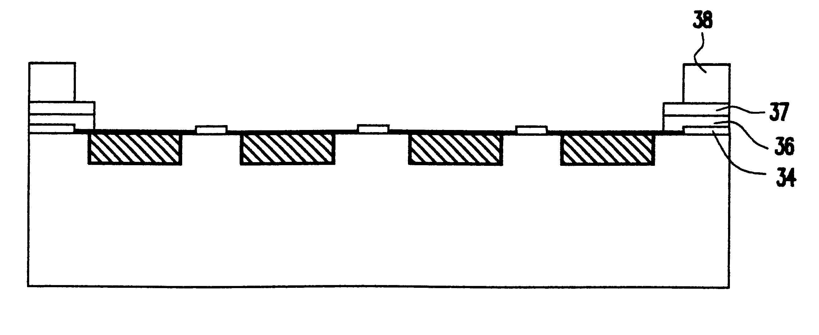
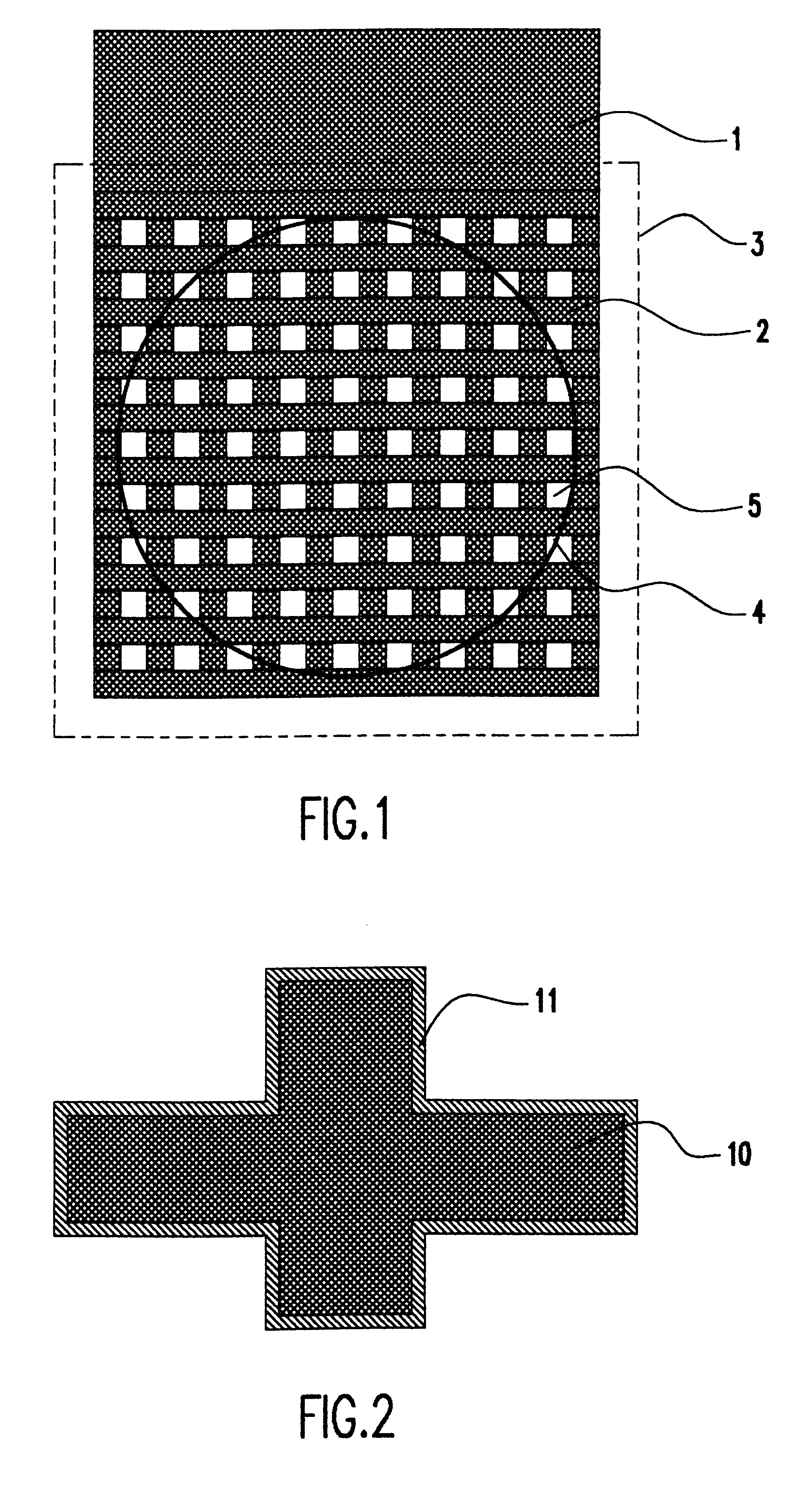
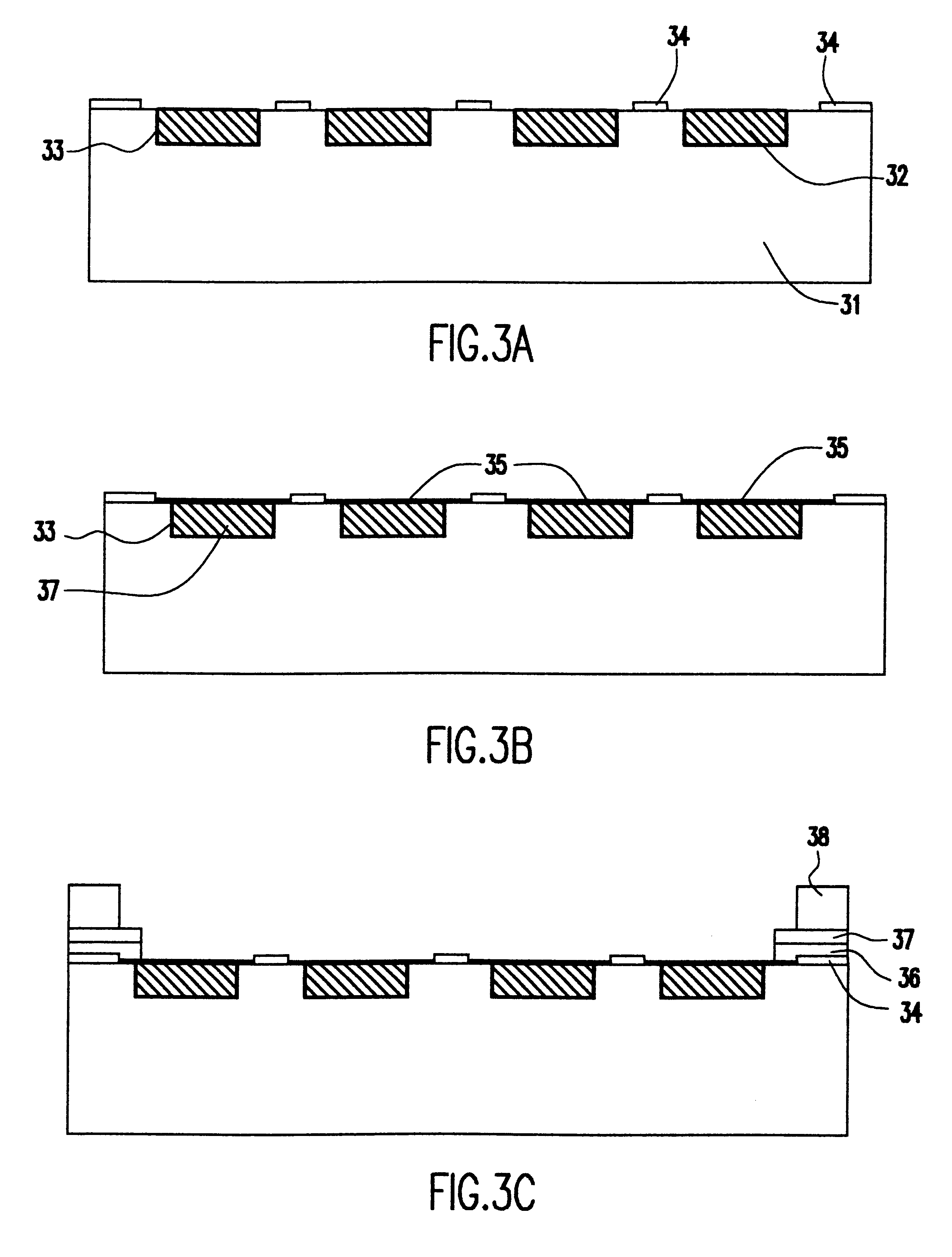
This invention makes use of an optimized pad design of the last metal copper pad structure. The structure is comprised of an array of silicon dioxide "pegs" arranged in a lattice work pattern throughout the damascene copper last-metal pad. The pegs provide supports to facilitate chemical mechanical polish (CMP) of the copper last metal and provide "islands" of good adhesion for a silicon nitride overlayer. Silicon dioxide peg size is large enough so that (after CMP of the copper last metal) a smaller peg of silicon nitride can be formed on top of the oxide peg using a non-critical block mask. For example, the silicon dioxide peg might be 10 .mu. square and the overlayer silicon nitride peg might be 7 .mu. square.

FIG. 1 shows an example of an orthogonal copper wiring mesh with pegs. By designing the nitride peg mask so that the nitride peg is contained within the oxide peg structure, a narrow overlap of a metal (or stack of metals having the properties that the metal has good adhesio...


PUM


Abstract

A controlled collapse chip connection (C4) structure having stronger resistance to failure is constructed for use with integrated circuit devices having copper wiring. Failure resistance is obtained by replacing the mechanically weak final passivation to copper interface. The weak interface is eliminated by use of a specific peg on peg structure together with a layer of shunt metal having excellent adhesion and barrier characteristics. A shunt metal, e.g., Ta or TaN, is placed between both the copper and final passivation and the copper and C4 metals such that it overlaps the edge of the peg defined wiring mesh to encase the copper. Overlap is obtained by the peg on peg structure where a SiO2 peg defines the copper wire mesh and a smaller Si3N4 peg placed on the SiO2 peg defines the overlap above the mesh wire and provides the ability to pattern the overlayer shunt without exposure of the copper conductor.

Description

1. Field of the InventionThe present invention generally relates to integrated circuit devices using copper wiring technology and more particularly to reducing failures at the interface between the last wiring level copper contact pad and the controlled collapse chip connect (C4) structure.2. Background DescriptionCopper back end of line (BEOL) wiring technologies offer substantial performance and potential cost advantages over the traditional aluminum technologies used for integrated circuit device fabrication. However, copper metalization is inherently more process-sensitive than aluminum, and less compatible with established chip / packaging interconnection technology. Copper metal readily forms a native oxide, which is not self-passivating like that of aluminum, but rather can continue to react in the presence of air and moisture to form corrosion products. Additionally, some inorganic dielectric materials, in particular silicon nitride, which are used as a barrier layer to preven...

Claims


Application Information

Patent Timeline
IPC IPC(8): H01L23/532H01L23/48H01L23/485H01L23/52
CPCH01L23/53238H01L24/02H01L2224/0401H01L2924/01013H01L2924/01014H01L2924/01018H01L2924/01022H01L2924/01027H01L2924/01029H01L2924/0105H01L2924/01073H01L2924/01074H01L2924/01082H01L2924/014H01L2924/04941H01L2924/04953H01L2924/05042H01L2924/14H01L2924/01033H01L2924/01072H01L24/05
Inventor DAUBENSPECK, TIMOTHYLUCE, STEPHEN E.MOTSIFF, WILLIAM
Owner IBM CORP
Why Eureka
Try Eureka