Electronic component mounted structure and method of manufacturing the same
- Summary
- Abstract
- Description
- Claims
- Application Information
AI Technical Summary
Benefits of technology
Problems solved by technology
Method used
Image

Examples
first embodiment
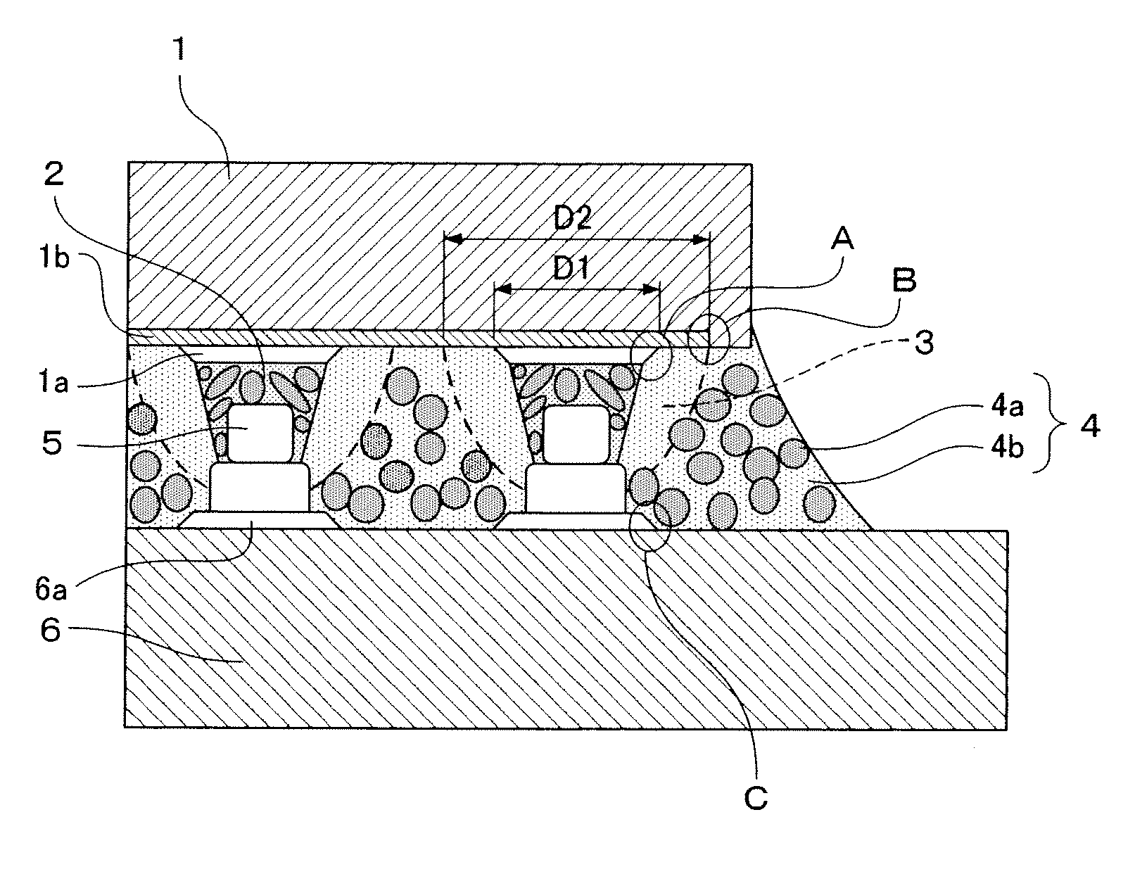
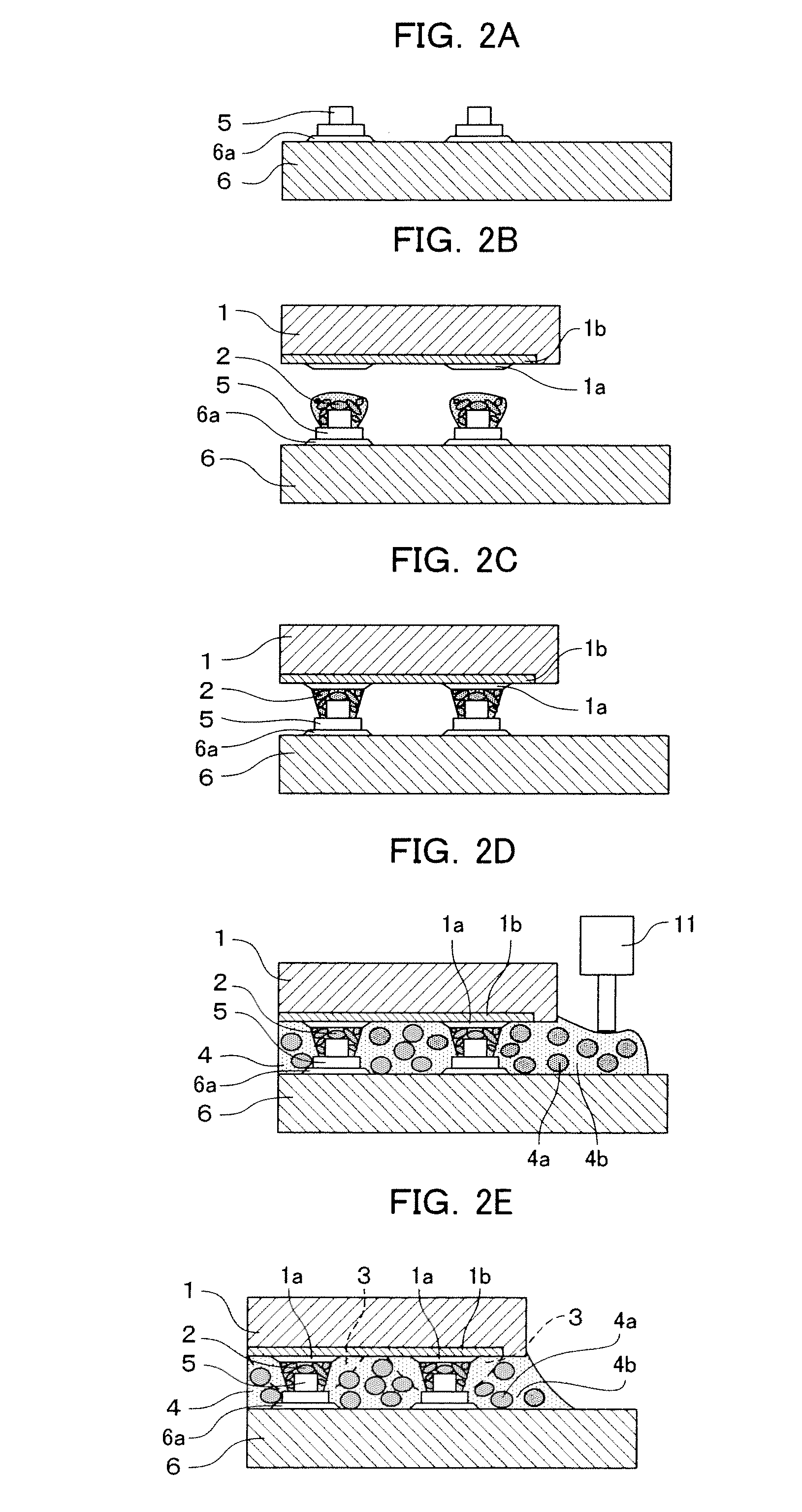
[0027]In the electronic component mounted structure shown in FIG. 1, a multi-layer wiring layer 1b consisting of a fine wiring layer and a fragile low-dielectric-constant insulating film (for example, a Low-k layer or Ultra low-k layer) is provided on the principal surface of a semiconductor element 1 which forms an electronic component, and a plurality of electrode terminals 1a are provided in an area arrangement on the uppermost surface thereof. This principal surface is called the “electrode surface” below.
[0028]A circuit substrate 6 on which the semiconductor element 1 is mounted (for example, a glass epoxy multi-layer substrate, an aramid multi-layer substrate, a silicon substrate) has electrode terminals 6a in an arrangement opposing the electrode terminals 1a of the semiconductor element 1, and metal projecting electrodes 5 (so-called “stud bumps”) are formed on each of the electrode terminals 6a. The electrode terminals 1a and 6a are made of gold, aluminum, nickel or copper,...
second embodiment
[0051]In the electronic component mounted structure shown in FIG. 3, similarly to the first embodiment, the semiconductor element 1 (hereinafter, called the “first semiconductor element 1”) comprises a multi-layer wiring layer 1b consisting of a fine wiring layer and a fragile low-dielectric-constant insulating film (for example, a Low-k layer or Ultra low-k layer) provided on the electrode surface, and a plurality of electrode terminals 1a are provided in an area arrangement on the uppermost surface thereof. A second semiconductor element 7 which is disposed so as to oppose the first semiconductor element 1 has electrode terminals 7a in an arrangement opposing the electrode terminals 1a, and a porous low dielectric constant insulating film 7b underneath the electrode terminals 7a.
[0052]The first electrode terminals 1a of the first semiconductor element 1 and the electrode terminals 7a of the second semiconductor element 7 are connected electrically and mechanically by means of a c...
third embodiment
[0057]The electronic component mounted structure shown in FIG. 4 is the same as that in the first embodiment, with the exception that projecting electrodes are not formed on the electrode terminals 6a of the circuit substrate 6. The electrode terminals 1a of the semiconductor element 1 and the electrode terminals 6a of the circuit substrate 6 are bonded together electrically and mechanically by means of a conductive adhesive 2.
[0058]A low elasticity layer 3 is formed about the periphery of each connecting section between an electrode terminal 1a and an electrode terminal 6a, and the low elasticity layer 3 covers the periphery of the conductive adhesive 2, the electrode surface about the periphery of the electrode terminal 1a and the electrode surface about the periphery of the electrode terminal 6a. Apart from this, a molding resin 4 is filled into the gap between the semiconductor element 1 and the circuit substrate 6. The materials of the conductive adhesive 2 and the molding resi...
PUM
| Property | Measurement | Unit |
|---|---|---|
| Length | aaaaa | aaaaa |
| Density | aaaaa | aaaaa |
| Electrical conductor | aaaaa | aaaaa |
Abstract
Description
Claims
Application Information
 - Generate Ideas
- Intellectual Property
- Life Sciences
- Materials
- Tech Scout
- Unparalleled Data Quality
- Higher Quality Content
- 60% Fewer Hallucinations
Browse by: Latest US Patents, China's latest patents, Technical Efficacy Thesaurus, Application Domain, Technology Topic, Popular Technical Reports.
© 2025 PatSnap. All rights reserved.Legal|Privacy policy|Modern Slavery Act Transparency Statement|Sitemap|About US| Contact US: help@patsnap.com