
Semiconductor device and method for manufacturing same

a technology of semiconductor devices and semiconductors, applied in semiconductor devices, electrical devices, transistors, etc., can solve the problems of difficult control of vsub>th/sub> of a fully depleted mos transistor to fall within either of the above ranges, and become difficult to control vsub>th/sub>to be a desired value, etc., to suppress the short-channel effect, low power, and high speed

Inactive Publication Date: 2009-10-08
NEC CORP
View PDF8 Cites 12 Cited by
  • Summary
  • Abstract
  • Description
  • Claims
  • Application Information

AI Technical Summary

Benefits of technology

[0021]As described above, a semiconductor device including a fully depleted MOS transistor including a metal gate electrode and a high-dielectric gate insulating film can operate at a low power level and improve mobility (operate at a higher speed) by lowering the channel dose. Lowering the channel dose, however, disadvantageously makes it difficult to control Vth.
[0039]To address the problem, the present inventor has intensively conducted studies on a variety of metal gate electrode materials and found that metal silicide having a specific composition may be preferably used as the gate electrode material of each of the pMOS and nMOS transistors. That is, the present inventor has found that in the thus configured semiconductor device, Vth values of the nMOS and pMOS transistors can be controlled to values necessary for a low-power device, resulting in a semiconductor device with excellent device characteristics and reliability.
[0089]It is possible to provide a MOS transistor that consumes a low power and can operate at a high speed (nMOS transistor, pMOS transistor, CMOS transistor). Specifically, a MOS transistor with suppressed short-channel effect and improved mobility by lowering channel dose in the semiconductor channel region, reduced parasitic capacitance and substrate leakage current, is to be formed.

Problems solved by technology

Lowering the channel dose, however, disadvantageously makes it difficult to control Vth.
Specifically, to achieve a low-power semiconductor device, it is necessary to set Vth of a pMOS transistor to a value ranging from approximately −0.6 to −0.3 V and Vth of an nMOS transistor to a value ranging from approximately 0.3 to 0.6 V. It is, however, very difficult to control Vth of a fully depleted MOS transistor to fall within either of the above ranges by using conventional MOS transistor technologies and the technologies disclosed in International Publication No. 2006 / 001271 and International Electron Device Meeting, Technical Digest, 2004, pp.
As a result, it becomes difficult to control Vth to be a desired value.
In particular, when a high-dielectric insulating film is used as the gate insulating film, the variation in work function further increases due to Fermi level pinning.
Therefore, in a silicide (metal gate) electrode formation method of related art in which a silicide film is deposited on a gate insulating film by using CVD or other methods, the variation of work function is large and it is difficult to control the composition of the gate electrodes in such a way that the pMOS and nMOS transistors have Vth values in a range necessary to achieve a stable low-power semiconductor device.

Method used


Image

  • Semiconductor device and method for manufacturing same
  • Semiconductor device and method for manufacturing same
  • Semiconductor device and method for manufacturing same

Examples


first exemplary embodiment

[0181]FIGS. 7 to 9 show an example of a method for manufacturing a semiconductor device of the present invention. FIGS. 7 to 9 show a method for manufacturing a semiconductor device including a planar pMOS transistor.

[0182]First, a substrate including support substrate 1, embedded insulating film 11, and silicon layer 42 with an n-type region is prepared. The thickness of silicon layer 42 in the substrate is adjusted in such a way that a manufactured pMOS transistor is fully depleted. The substrate can be formed by using bonding or SIMOX. For example, a smart-cut method or an ELTRAN method may be used.

[0183]STI (Shallow Trench Isolation) technique is then used to form isolation region 2 in silicon layer 42 so that n-type region 24 is isolated. Thermal oxidation is then used to form insulating film 19 comprised of a silicon oxide film on the surface of silicon layer 42.

[0184]High-dielectric insulating film 18 is subsequently formed on insulating film 19. To form an HfSiON film as hig...

second exemplary embodiment

[0203]FIGS. 10 to 14 show another example of the method for manufacturing a semiconductor device of the present invention. FIGS. 10 to 14 show a method for manufacturing a semiconductor device including planar pMOS and nMOS transistors.

[0204]First, a substrate including support substrate 1, embedded insulating film 11, and silicon layer 42 with n-type and p-type regions is prepared. The thickness of silicon layer 42 in the substrate is adjusted in such a way that each of manufactured MOS transistors is fully depleted.

[0205]Isolation region 2 is then formed so that n-type region 24 is isolated from p-type region 23, as in the first exemplary embodiment. Silicon oxide film 19, high-dielectric insulating film 18, poly-Si film (polysilicon film) 43, and mask layer 15 are sequentially formed on the surface of silicon layer 42 (FIG. 10(a)).

[0206]Patterning is then carried out to form a region comprised of a first gate insulating film, first gate electrode material 14b, and mask (D) 15b on...

third exemplary embodiment

[0215]FIG. 16 shows a variation of the first exemplary embodiment. The present exemplary embodiment differs from the first exemplary embodiment in that the present exemplary embodiment relates to a method for manufacturing a semiconductor device in which each of the first and second gate electrodes is comprised of two layers and the top layer is a low-resistance layer. First, after the same steps as those in the first exemplary embodiment are carried out for the steps that correspond to FIG. 12(b) and the earlier figures, sputtering is used to deposit Si layer 52 all over the resulting surface (FIG. 16(a)). Heat treatment is then carried out to cause the Ni2Si or Ni3Si crystalline phase that forms the second gate electrode (silicide region (2)) to react with the Si. In this process, Si is thermally diffused only into the upper portion of the second gate electrode by adjusting the period of the heat treatment, and only the upper portion of the second gate electrode becomes low-resist...


PUM


Abstract

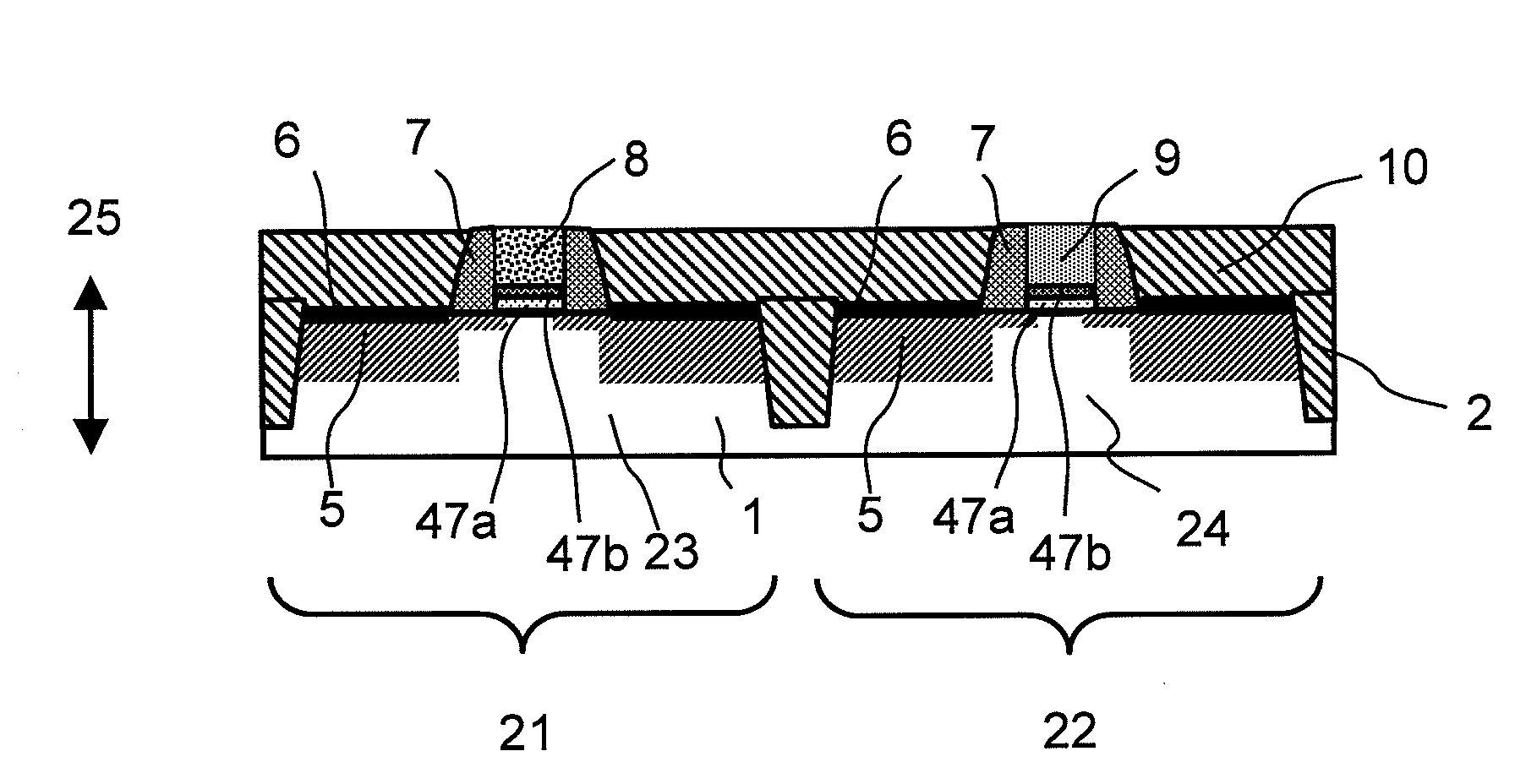
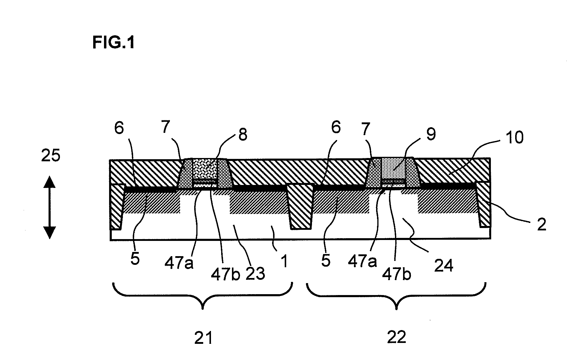
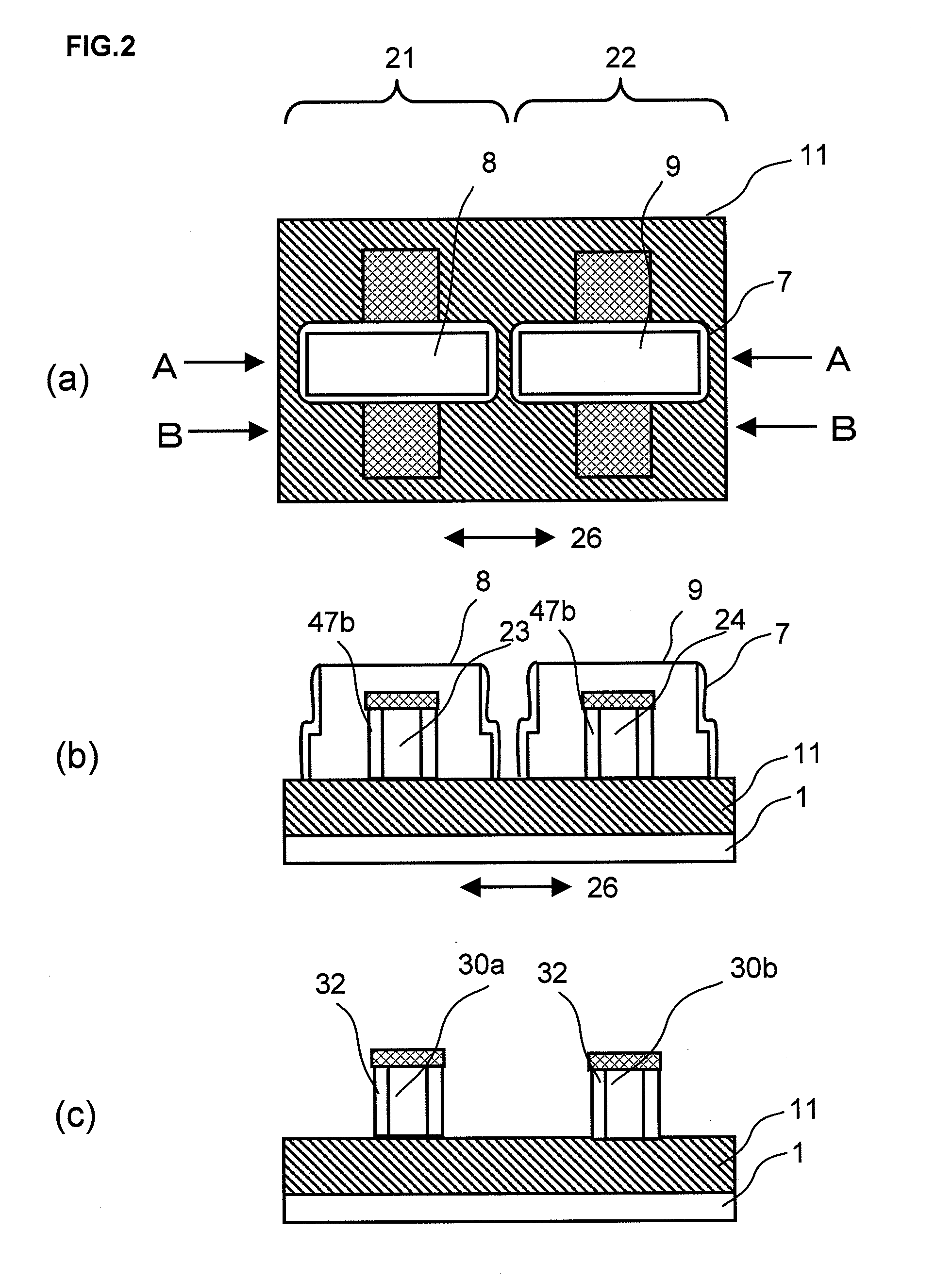
There is provided a semiconductor device having excellent device characteristics and reliability in which Vth values of an nMOS transistor and a pMOS transistor are controlled to be values necessary for a low-power device. The semiconductor device includes a pMOS transistor and an nMOS transistor formed by using an SOI substrate. The pMOS transistor is a fully depleted MOS transistor including a first gate electrode comprising at least one type of crystalline phase selected from the group consisting of a WSi2 crystalline phase, an MoSi2 crystalline phase, an NiSi crystalline phase, and an NiSi2 crystalline phase as silicide region (1). The nMOS transistor is a fully depleted MOS transistor comprising at least one type of crystalline phase selected from the group consisting of a PtSi crystalline phase, a Pt2Si crystalline phase, an IrSi crystalline phase, an Ni2Si crystalline phase, and an Ni3Si crystalline phase as silicide region (2).

Description

TECHNICAL FIELD[0001]The present invention relates to a fully depleted nMOS transistor and pMOS transistor fabricated by using an SOI substrate, a semiconductor device including the two MOS transistors, and a method for manufacturing the same.[0002]The present invention also relates to a low-power semiconductor device in which Vth (threshold voltage) values of the MOS transistors are controlled to provide excellent device characteristics, and a method for manufacturing the same.BACKGROUND ART[0003]As transistors have been continuously miniaturized, there have been problems of reduction in drive current (Ion) due to depletion of a polysilicon electrode and increase in gate leakage current due to reduction in thickness of a gate insulating film. To address such problems, there has been a proposal of a MOS transistor that prevents depletion of the gate electrode by using a metal gate electrode made of a metal or other materials and that uses high-dielectric insulating film as a gate in...

Claims


Application Information

Patent Timeline
Patent Type & Authority Applications(United States)
IPC IPC(8): H01L27/088H01L29/786H01L21/336H01L21/8238H01L21/8236H01L27/092
CPCH01L21/28097H01L21/823835H01L21/823842H01L21/823878H01L29/785H01L27/1203H01L29/4908H01L29/4975H01L29/66545H01L21/84H01L21/845H01L27/1211H01L29/66803H01L21/18H01L21/20
Inventor TAKAHASHI, KENSUKE
Owner NEC CORP
Learn More