Thin seeded Co/Ni multilayer film with perpendicular anisotropy for spintronic device applications

a multi-layer film, perpendicular anisotropy technology, applied in the direction of instruments, record information storage, transportation and packaging, etc., can solve the problems of inability to integrate devices, all literature examples suffer from at least one drawback, and the use of external magnetic fields generated by current carrying lines to switch the magnetic moment direction becomes problematic, etc., to minimize the impinging ion energy, the effect of high inert gas pressure and maximize the pma property

Active Publication Date: 2009-10-15
TDK CORPARATION +1
View PDF9 Cites 218 Cited by
  • Summary
  • Abstract
  • Description
  • Claims
  • Application Information

AI Technical Summary

Benefits of technology

[0014]One objective of the present invention is to provide a thin seed layer for a laminated (Co / Ni)x reference layer in a spin valve of a spintronic device that fully establishes the perpendicular magnetic anisotropy (PMA) in the (Co / Ni)x stack without causing spin depolarization or requiring a heat treatment that could degrade other components in the device.
[0018]In a third embodiment, the Cu spacer in the aforementioned bottom spin valve configuration is modified by inserting a confining current path (CCP) nano-oxide layer (NOL) between upper and lower portions of the Cu spacer. For example, an amorphous oxide such as AlOx may be formed between two copper spacer layers in a Cu / AlOx / Cu configuration. In a CCP-CPP scheme, the Cu metal path is limited through an insulator template so that the MR ratio in the spin valve can be enhanced quite significantly.
[0022]An important feature of all embodiments is that each of the Co and Ni layers in the (Co / Ni)x laminate is deposited with a very low RF power and a high inert gas pressure to minimize the impinging ion energy so that deposition of a layer does not damage the Co or Ni layer on which it is formed. Thus, the interfaces between the Co and Ni layers are preserved to maximize the PMA property. Furthermore, this method enables the PMA of (Co / Ni)x laminates to be preserved with a substantially thinner seed layer.

Problems solved by technology

As the size of MRAM cells decreases, the use of external magnetic fields generated by current carrying lines to switch the magnetic moment direction becomes problematic.
As a result, spin valve structures based on PMA are capable of scaling for higher packing density which is one of the key challenges for future MRAM applications and other spintronic devices.
However, all of the literature examples suffer from at least one drawback.
Unfortunately, FePt or Tb(Fe)Co need high temperature annealing to achieve high enough PMA which is unacceptable for device integration since certain components are damaged by high temperatures.
CoPt and its alloys such as CoCrPt and CoPt—SiO2 are not desirable because Pt and Cr are severe spin depolarizing materials and will seriously quench the amplitude of spintronic devices if incorporated in the spinvalve structures.
As stated above, Co / Pt, Co / Pd, and Co / Ir will not be good PMA materials for spintronic devices because of the severe spin depolarizing property of Pt, Pd, and Ir.
Furthermore, Co / Pt, Co / Pd, and Co / Ir configurations typically require a very thick and expensive Pt, Pd, or Ir as a seed layer.
Au is associated with high cost and easy interdiffusion to adjacent layers which makes a Co / Au multilayer for PMA purposes less practical.
er. The aforementioned seed layers are not practical with Co / Ni multilayer PMA configurations in spintronic devi
ance. Seed layers thicker than about 100 Angstroms will require thinning a different layer in the spin valve to maintain a certain minimum thickness for the spin valve which can easily lead to performance degrad

Method used


Image

  • Thin seeded Co/Ni multilayer film with perpendicular anisotropy for spintronic device applications
  • Thin seeded Co/Ni multilayer film with perpendicular anisotropy for spintronic device applications
  • Thin seeded Co/Ni multilayer film with perpendicular anisotropy for spintronic device applications

Examples


example 1

[0059]An experiment was conducted to demonstrate the effectiveness of forming a (Co / Ni)x laminated reference layer in minimizing the required thickness of the seed layer in a spin valve stack. A partial spin valve stack comprised of a Cu seed layer, (Co / Ni)20 laminated layer where each Co layer is 2 Angstroms thick and each Ni layer is 4 Angstroms thick, and a Ru10 / Ta40 / Ru30 cap layer was fabricated in order to obtain PMA values from MH curves using a vibrating sample magnometer (VSM). The thickness of each layer in the composite cap layer is shown by the number following each of the elements. Copper seed layer thickness was reduced from 1000 Angstroms in FIG. 6a to 500 Angstroms in FIG. 6b, 200 Angstroms in FIG. 6c, and to 100 Angstroms in FIG. 6d. The upper plot in each figure shows the horizontal to plane component of each magnetic field and the lower plot in each figure illustrates the perpendicular magnetic anisotropy (PMA) component. It should be understood that the distances ...

example 2

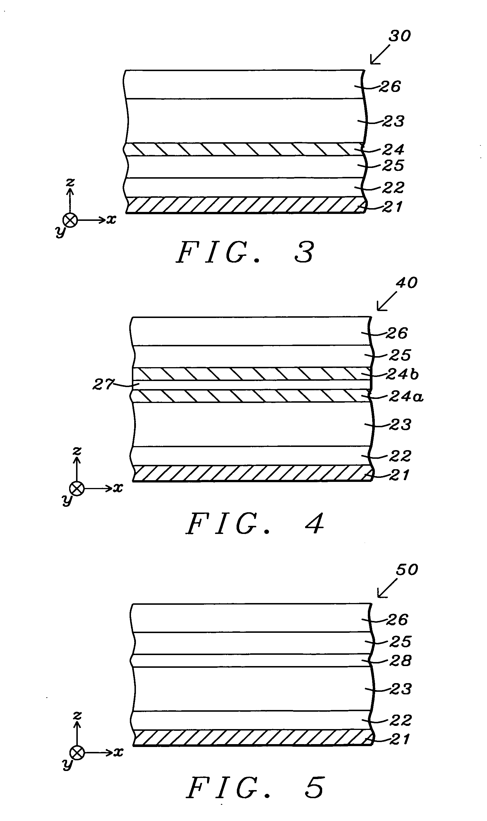
[0060]In a second experiment, a Ta / Ru underlayer was inserted to form a Ta / Ru / Cu seed layer and further enhance the (111) texture of the upper Cu layer according to an embodiment of the present invention. The lower Ta layer thickness is 30 Angstroms and the middle Ru layer thickness is 20 Angstroms. The other layers in the partial spin valve stack have the same composition and thickness as indicated in the previous example. As a result, PMA is further improved with respect to FIGS. 6a-6d as indicated by the MH curves in FIGS. 7a-7d. Note that the distance s5 in FIG. 7c is greater than s4 where the Cu layer in both cases is 100 Angstroms thick. Those skilled in the art will also recognize that the sloped portions of the curves in FIGS. 7a-7d are more vertical than the sloped portions in FIGS. 6a-6d which represents improved perpendicular magnetic properties. The thickness of the upper Cu layer in the composite seed layer is reduced from 2000 Angstroms in FIG. 7a, to 200 Angstroms in ...

example 3

[0061]To further explore the effect of thinning the upper Cu layer in the composite seed layer described in Example 2, the upper Cu layer was thinned from 50 Angstroms in FIG. 8a to 30 Angstroms in FIG. 8b, and completely removed in FIG. 8c. Note that the resulting seed layer has a 30 Angstrom thick Ta layer and a 50 Angstrom thick Ru layer in the Ta / Ru configuration. In addition, the thickness of each Ni layer in the (Co / Ni)20 stack was increased slightly to 5 Angstroms. We have found that excellent PMA properties are retained in the (Co / Ni)20 multilayer even when the Cu layer in the composite seed layer is removed as illustrated in FIG. 8c.


PUM

PropertyMeasurementUnit
thicknessaaaaaaaaaa
thicknessaaaaaaaaaa
thicknessaaaaaaaaaa

Abstract

A spin valve structure for a spintronic device is disclosed and includes a composite seed layer made of at least Ta and a metal layer having a fcc(111) or hcp(001) texture to enhance perpendicular magnetic anisotropy (PMA) in an overlying (Co / Ni)x multilayer. The (Co / Ni)x multilayer is deposited by a low power and high Ar pressure process to avoid damaging Co / Ni interfaces and thereby preserving PMA. As a result, only a thin seed layer is required. PMA is maintained even after annealing at 220° C. for 10 hours. Examples of GMR and TMR spin valves are described and may be incorporated in spin transfer oscillators and spin transfer MRAMs. The free layer is preferably made of a FeCo alloy including at least one of Al, Ge, Si, Ga, B, C, Se, Sn, or a Heusler alloy, or a half Heusler alloy to provide high spin polarization and a low magnetic damping coefficient.

Description

RELATED PATENT APPLICATION[0001]This application is related to the following: Docket #HMG07-042, Ser. No. 12 / 079,445, filing date Mar. 27, 2008; herein incorporated by reference in its entirety.FIELD OF THE INVENTION[0002]The invention relates to a high performance spin valve such as a CPP-GMR (current perpendicular to plane-giant magnetoresistance) element or a magnetic tunnel junction (MTJ) and a method for making the same, and in particular, to a memory device that includes a spin valve structure having a composite seed layer with (111) texture to induce a preferred (111) orientation in an overlying laminated Co / Ni reference layer and thereby enhance perpendicular magnetic anisotropy (PMA) therein.BACKGROUND OF THE INVENTION[0003]Magnetoresistive Random Access Memory (MRAM), based on the integration of silicon CMOS with MTJ technology, is a major emerging technology that is highly competitive with existing semiconductor memories such as SRAM, DRAM, and Flash. Similarly, spin-tran...

Claims


Application Information

Patent Timeline
Patent Type & Authority Applications(United States)
IPC IPC(8): G11B5/33B05D5/00C23C14/35
CPCG01R33/098Y10T428/1129G11C11/16Y10T428/1136Y10T428/1114Y10T29/49044Y10T29/49048Y10T428/1121Y10T29/49032Y10T29/49043Y10T428/1107Y10T29/49052Y10T428/1143Y10T29/49046G01R33/1284G11C11/161H10N50/85H10N50/10
Inventor ZHANG, KUNLIANGLI, MINZHOU, YUCHENOIKAWA, SOICHIYAMADA, KENICHIROKOUI, KATSUHIKO
Owner TDK CORPARATION
Why Eureka
Try Eureka