

Film forming composition for nanoimprinting and method for pattern formation
a technology of nano-imprinting and composition, which is applied in the field of nano-imprinting composition and composition for pattern formation, can solve the problems of high initial cost of exposure devices, high cost of masks with such a micro-shape, and high cost of exposure devices used for optical exposure lithography techniques, so as to prevent the separation of transfer patterns, eliminate the problem of holding time on the substrate, and improve the effect of etching resistan
Inactive Publication Date: 2009-10-22
TOKYO OHKA KOGYO CO LTD
View PDF0 Cites 43 Cited by
- Summary
- Abstract
- Description
- Claims
- Application Information
AI Technical Summary
Benefits of technology
[0057]According to the film-forming composition for the nanoimprinting of the present invention, it is possible to realize the nanoimprint lithography, while exerting the advantages of both of the photo-nanoimprint lithography and the room-temperature nanoimprint lithography, as well as eliminating the problems of both of them. That is, according to the film-forming composition of the present invention, it is possible to obtain a resist, which has excellent resistance to etching with an oxygen gas, prevents separation of the transfer pattern, eliminates the problem about the holding time on the substrate, and has excellent transferability. Furthermore, the resist formed with the film-forming composition of the present invention has excellent resistance to etching with gases other than the oxygen gas. This broadens a range of selection of an etching gas, thereby making it possible to form a pattern on a substrate independently of a particular kind of gas.
Problems solved by technology
However, since devices used for the optical exposure lithography techniques are expensive, initial cost for the exposure devices has been increased with the further miniaturization.
Moreover, a mask for obtaining a high resolution at the same level as a light wavelength is necessary for the optical exposure lithography, and the mask having such a microshape has been expensive.
Furthermore, since the demand for higher integration is limitless, further miniaturization is required.
However, the thermal cycle nanoimprint lithography has problems such as reduction of the throughput due to the time taken by heating-up and cooling of the resist, dimensional change and reduction of the precision of the transfer pattern due to the temperature difference, and reduction of the alignment due to the thermal expansion.
Method used
View moreImage
Smart ImageViewing Examples

Examples
example 1
[0139]1 mol of tetraethoxysilane, 0.5 mol of monoacryloxypropyltrimethoxysilane, and 0.5 mol of monovinyltrimethoxysilane were dissolved in 170 g of isopropyl alcohol. Subsequently, 190 g of pure water and 0.02 g of concentrated nitric acid were added thereto, and the mixture was stirred at the room temperature for six hours. The obtained composition was diluted with isopropyl alcohol so that the solid content in terms of SiO2 became 7%. Subsequently, to 100 g of the obtained liquid, 1 g of IRGACURE-369 (produced by Ciba Specialty Chemicals: 2-benzyl-2-dimethylamino-1-(4-morpholinophenyl)-butan-1-one) was added as a photopolymerization initiator, thereby preparing an application liquid.
Login to View More PUM
| Property | Measurement | Unit |
|---|---|---|
| Pressure | aaaaa | aaaaa |
| Composition | aaaaa | aaaaa |
| Molecular weight | aaaaa | aaaaa |
Abstract
This invention provides a film forming composition for nanoimprinting, which has excellent resistance to etching with oxygen gas, can prevent the separation of a transfer pattern, can eliminate a problem of a holing time on a substrate, and is also excellent in transferability, and photosensitive resist, a nanostructure, a method for pattern formation using the same, and a program for realizing the method for pattern formation. The film forming composition for nanoimprinting comprises a polymeric silicon compound having the function of causing a photocuring reaction. Preferably, the polymeric silicon compound has a functional group cleavable as a result of response to electromagnetic waves and causes a curing reaction upon exposure to electromagnetic waves. More preferred are siloxane polymer compounds, silicon carbide polymer compounds, polysilane polymer compounds, and silazane polymer compounds, or any mixture thereof.
Description
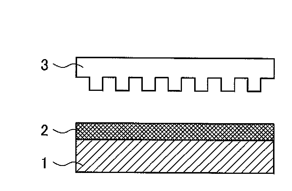
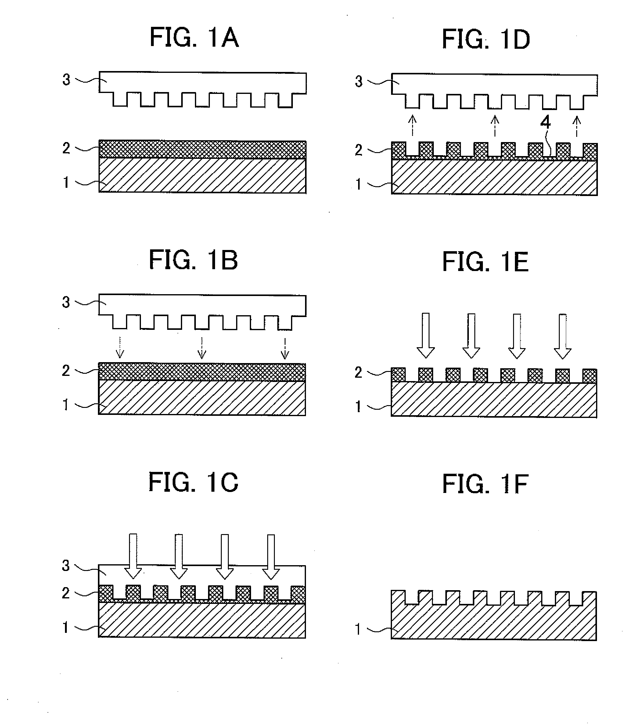
TECHNICAL FIELD[0001]The present invention relates to a film-forming composition for nanoimprinting and a method for pattern formation using the same. More particularly, the present invention relates to a film-forming composition and a photosensitive resist for nanoimprinting, which are provided with a function to cause photocuring reaction, as well as a nanostructure, a method for pattern formation using the same, and a program for realizing the method for pattern formation.BACKGROUND ART[0002]A lithography technology is a core technology of semiconductor device processes, and the electric wiring is further miniaturized with higher integration of the recent semiconductor integrated circuits (IC). Especially, in a semiconductor integrated circuit (IC) as referred to as a very large scale integrated circuit (VLSI), integration degree of elements surpasses 10,000,000, therefore a fine pattern lithography technique is essential.[0003]As the fine pattern lithography technique for realiz...
Claims
Login to View More Application Information
Patent Timeline
 IPC IPC(8): B32B3/10C08G77/14C08L83/06C08J3/28B32B38/06
CPCB82Y10/00B82Y40/00C08G77/20C09D183/04Y10T428/24802G03F7/0757H01L21/0273Y10T156/1041G03F7/0002G03F7/035B29C59/02B82B1/00B82B3/00
InventorSAKAMOTO, YOSHINORIYAMASHITA, NAOKIISHIKAWA, KIYOSHI
OwnerTOKYO OHKA KOGYO CO LTD