Pellicle and method for producing pellicle

a technology of pellicle and euv, which is applied in the field of pellicle for lithography, can solve the problems of many technical problems which have to be solved for realization of pellicle for euv, pattern width of 32 nm or less, and difficulty in meeting patterning, etc., and achieves excellent mechanical and chemical stability, reduces cracks, and transmission high

Active Publication Date: 2009-11-05
SHIN ETSU CHEM IND CO LTD
View PDF8 Cites 23 Cited by
  • Summary
  • Abstract
  • Description
  • Claims
  • Application Information

AI Technical Summary

Benefits of technology

[0025]In the present invention, the silicon single crystal film having a crystal plane as its principal plane, the crystal plane being inclined at 3 to 5° from any lattice plane belonging to {100} planes or {111} planes is used as a pellicle film, and therefore this configuration provides stability when various mechanical and chemical treatments such as stripping, polishing and etching at the time of for

Problems solved by technology

However, in such lithography based on the excimer exposure technologies, it is regarded as difficult to meet patterning requiring further miniaturization with a pattern width of 32 nm or less.
Among these, development for the light source and resist has been already made substantial progress, whereas for pellicle, many technical problems which have to be solved for realization of a pellicle for EUV remain unsolved.
However, the prospects for resolution of problems of such high transmission and chemical stability, and further the material development for a practical pellicle film having an excellent fabrication yield are still far from certain at present.
However, silicon used as a pellicle film in Non-Patent Document 1 is a film deposited by a sputtering method or the like, and therefore necessarily become amorphous, inevitably resulting in the high absorption coefficient and low transmitta

Method used


Image

  • Pellicle and method for producing pellicle
  • Pellicle and method for producing pellicle
  • Pellicle and method for producing pellicle

Examples


example 1

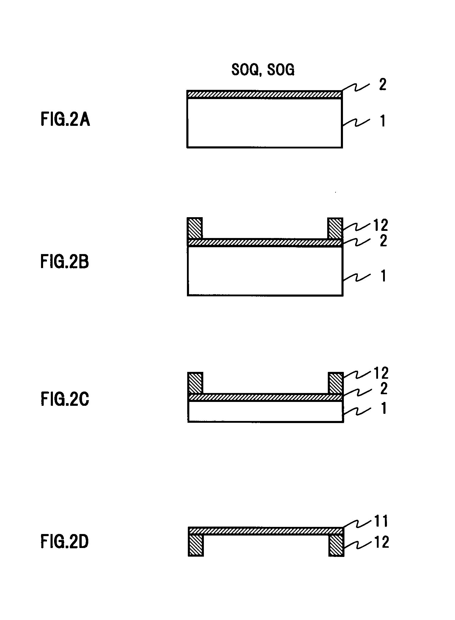
[0057]FIGS. 2A to 2D and FIGS. 3A to 3D are views for explaining a process example of a method of producing a pellicle of the present invention. FIGS. 2A to 2D are the views for explaining the process example with an SOQ (Silicon On Quartz) substrate or an SOG (Silicon On Glass) substrate used as an SOI substrate in a broad sense. FIGS. 3A to 3D are the views for explaining the process example with an SOI (Silicon On Insulator) substrate in a limited sense used as an SOI substrate in a broad sense.

[0058]In the case where the SOI substrates in a broad sense are an SOQ (Silicon On Quartz) substrate and an SOG (Silicon On Glass) substrate, support substrates 1 were a quartz substrate and a glass substrate, respectively. A support substrate 1 of the SOI (Silicon On Insulator) substrate in a limited sense was a substrate provided with, on its surface, an oxide film 1b on a silicon substrate 1a.

[0059]The principal planes of these support substrates each were provided with a silicon singl...

example 2

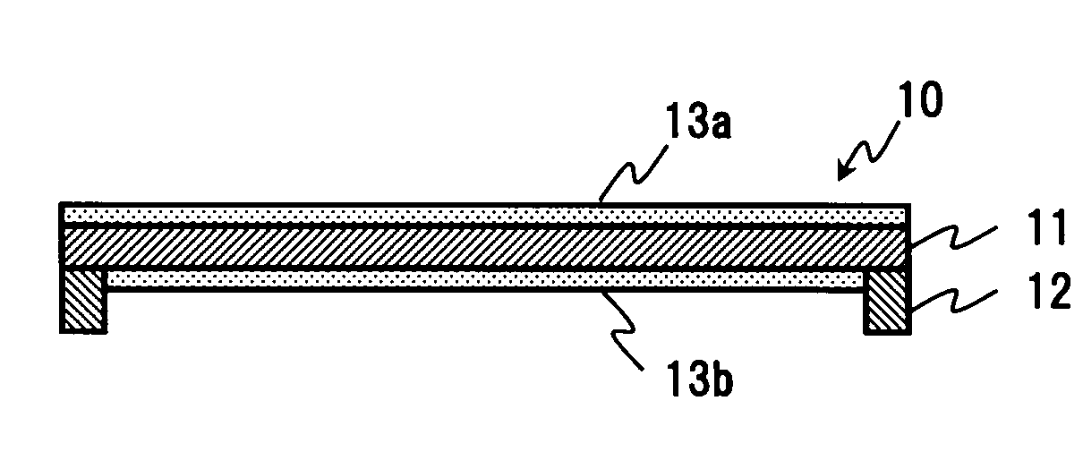
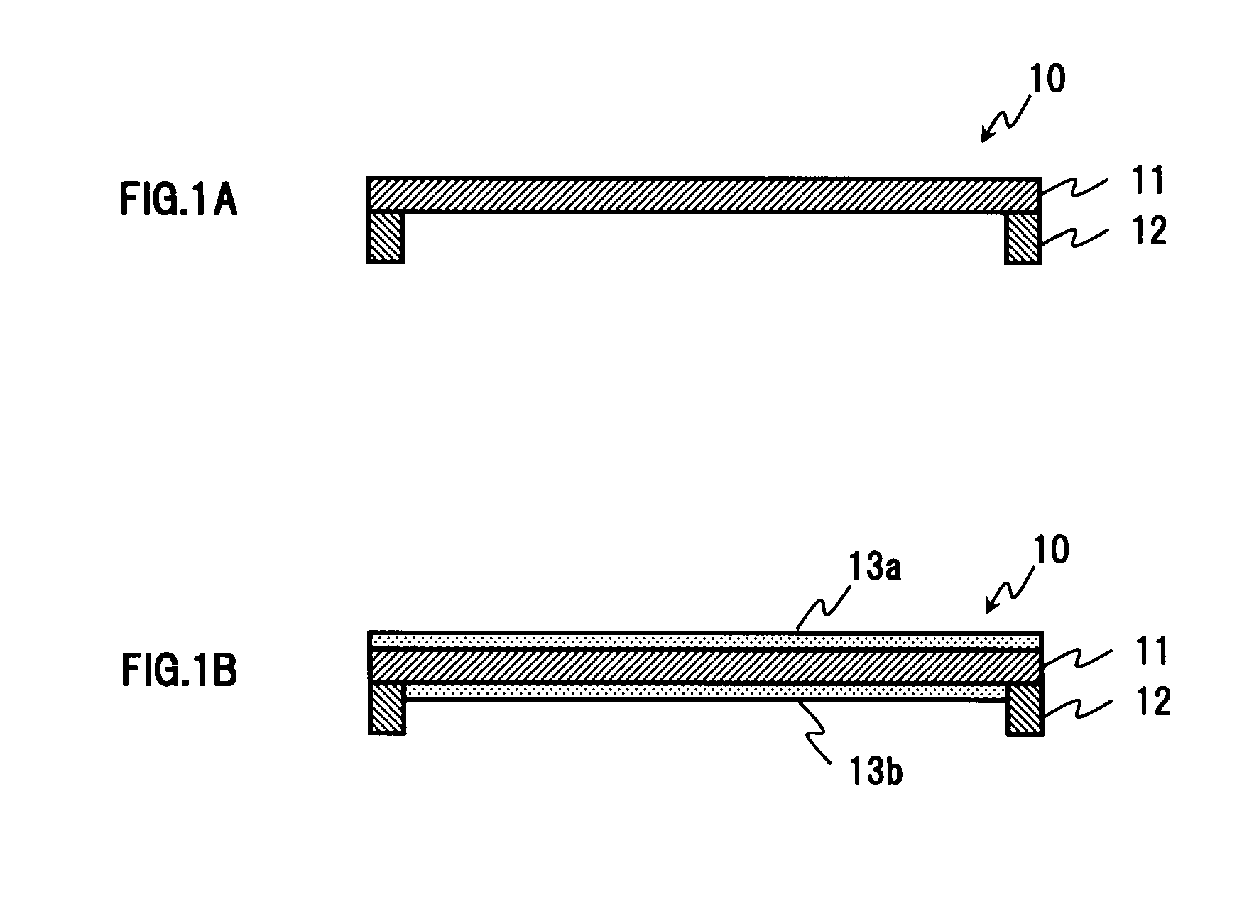
[0068]According to processes shown in FIGS. 2A to 2D and FIGS. 3A to 3D, the pellicle film 11 of a silicon single crystal film having an orientation plane as its principal plane, the orientation plane with a crystal orientation inclined at 3 to 5° (3° off to 5° off) from to direction, the pellicle film 11 being supported by the pellicle frame 12, was obtained.

[0069]The pellicle film 11 of the silicon single crystal film of the EXAMPLE had a thickness of 20 nm. Then, a SiC thin film having a thickness of a few nm was deposited on each of the front surface and back surface of the pellicle film 11 by gas cluster ion beam evaporation method to coat the pellicle film 11 of the silicon single crystal film.

[0070]It was confirmed that every pellicle obtained by EXAMPLE 1 and EXAMPLE 2 had transmittance of EUV light of 50% or more, and throughput during EUV exposure that was on a practical level, and showed no degradation of yield of the device due to foreign matters at all.

[0071]In the ab...


PUM


Abstract

A silicon single crystal film having a crystal plane as its principal plane, the crystal plane being inclined at 3 to 5° from any lattice plane belonging to {100} planes or {111} planes is used as a pellicle film. The silicon single crystal having such a crystal plane as its principal plane has effective bond density and Young's modulus thereof which are about 40% to about 50% higher than those of a silicon single crystal with <100> orientation, and therefore a cleavage and crack do not easily occur. Moreover, the silicon single crystal has a high chemical resistance such as hydrofluoric acid resistance, and hardly causes an etch pit and void. Accordingly, the present invention can provide a pellicle comprising a pellicle film for EUV having high transmission, and excellent mechanical and chemical stability, as well as having a high yield, and being practical also in cost.

Description

[0001]This application claims priority from Japanese Patent Application No. 2008-120664 filed May 2, 2008, which is incorporated hereinto by reference in its entirely.BACKGROUND OF THE INVENTION[0002]1. Field of the Invention[0003]The present invention relates to a pellicle for lithography. More particularly, the present invention relates to a pellicle suitable for lithography using extreme ultra violet (EUV) light, and a method for producing the same.[0004]2. Description of the Related Art[0005]With high integration of semiconductor devices, patterns formed by lithography are microminiaturized, and currently devices having a pattern width of about 45 nm are being put to practical use. Such a narrow line pattern can be realized by lithography based on a manner such as an ArF immersion method and a double exposure method which are improved techniques of conventional excimer exposure technologies.[0006]However, in such lithography based on the excimer exposure technologies, it is rega...

Claims


Application Information

Patent Timeline
IPC IPC(8): G03F1/00G03F1/22G03F1/24G03F1/62
CPCB82Y10/00G03F1/62G03F1/24B82Y40/00
Inventor KUBOTA, YOSHIHIROAKIYAMA, SHOJISHINDO, TOSHIHIKO
Owner SHIN ETSU CHEM IND CO LTD
Why Eureka
Try Eureka